
4 layers170 × 101 mm

 lk-ek/SC440_Preamp
SC440 OPA1678 microphone preamp
SC440 Preamp is an open-source printed circuit board by lk-ek, from the lk-ek/SC440_Preamp repository on GitHub. It is a 2-layer board of 30 × 35 mm with 29 parts on 14 nets, routed with 115 tracks and 6 vias.
It is built around the OPA1678IDRGR. Its parts include 10 resistors, 9 capacitors, 2 connectors and 1 IC. It belongs with the audio and music boards of this library.
Caveat: measurements show that the theoretical use for this preamp is a reduction of the noise floor by a whopping 0.2dB. The noise seems to come from either the capsule or the analog board.
So this is a nice flex mod as an exercise in analogue circuitry, but don't expect any quality gains from it at all.
A 5 V analog gain board for the t.bone SC 440 USB microphone. It sits between its original microphone/JFET board and USB/ADC board, AC-couples the signal, rebiases it around a buffered half-supply reference, and adds selectable gain. The aim is to use less gain in the following ADC stage. A reduction in overall recording noise depends on how much noise that stage contributes; microphone and original analog-board noise are amplified along with the signal.
Default in the current KiCad files: amplifier gain +10.10 dB, using R8 = 2.2 kΩ and R9 = 1 kΩ, with the C2 = 1 µF MLCC input option. C1, R1 and R2 are DNP. C9 = 330 pF is populated across R8.
The board outline is 30 × 35 mm, with 2 mm corner radii. PCB thickness in this project is 1.6 mm. Files were saved with KiCad 10.99 nightly; use a build that supports their file format.
The non-inverting amplifier uses Av = 1 + R8/R9, with R9 fixed at 1 kΩ.
Populate one R8 value; these are alternatives, not additional resistors.
| Variant | R8 | R9 | Voltage gain | Gain | Concrete R8 example, Yageo thin film |
|---|---|---|---|---|---|
| 6 dB | 1 kΩ | 1 kΩ | 2.0× | +6.02 dB | RT0805BRD071KL |
| 8 dB | 1.5 kΩ | 1 kΩ | 2.5× | +7.96 dB | RT0805BRD071K5L |
| 10 dB — CAD default | 2.2 kΩ | 1 kΩ | 3.2× | +10.10 dB | RT0805BRD072K2L |
The table gives the amplifier gain. End-to-end gain from J2 pin 4 to J1 pin 4 is slightly lower: R4/R6 alone introduce about 0.086 dB attenuation. The unloaded AC model gives approximately 5.93 / 7.87 / 10.01 dB at 1 kHz for the default MLCC option. See SIMULATION_VALIDATION.md for both capacitor options and the 20 kHz results.
These parts are 0805, 0.1%, 25 ppm/°C, 0.125 W. Ordinary 1% resistors also work; thin film is preferred for R8/R9 for ratio stability and low excess noise. Thin film does not eliminate thermal noise. The lower resistance values reduce that contribution compared with the older 22 kΩ/10 kΩ pair.
Use 6 dB where input-level headroom matters most; 10 dB provides the greatest analog boost. For a fixed ADC clipping level, allowable microphone-board input amplitude is inversely proportional to the selected voltage gain. Reduce ADC gain to obtain comparable recording levels, then check loud speech and plosives. An analog booster does not increase the ADC's full-scale voltage.
C9 remains 330 pF for all three variants. Its feedback-network pole is approximately 482 kHz / 322 kHz / 219 kHz for 6 / 8 / 10 dB respectively. This reduces the ideal amplifier gain toward unity at high frequencies; it is not a filter whose gain falls to zero. Its calculated contribution at 20 kHz is only about −0.006 / −0.014 / −0.032 dB respectively, before other circuit roll-off.
Choose exactly one of the following assemblies. The input resistor R4 and bias resistor R6 are unchanged for either option.
| Part | A — compact MLCC, CAD default | B — film |
|---|---|---|
| C2 | 1 µF, 0805, X7R, ≥16 V | DNP |
| C1 | DNP | 2.2 µF PET film, Faratronic C241J225J2SC000, 63 V, 5 mm pitch |
| R1, R2 | DNP | 0 Ω each, 0805 |
| R4 | 1 kΩ | 1 kΩ |
| R6 | 100 kΩ | 100 kΩ |
| Approximate input high-pass pole | 1.6 Hz | 0.72 Hz |
The default path is C2 → R4 → IN_AC. The film path is R1 → C1 → R2 → R4 → IN_AC. Do not populate both coupling branches: the two capacitors would operate in parallel rather than select a single option.
Both coupling capacitors are non-polarized. Film avoids the ferroelectric voltage dependence and microphony of X7R, but takes more space. The MLCC option is the compact assembly; its effective capacitance depends on the exact part and bias. These differences do not by themselves establish an audible benefit in the complete microphone.
The film variant requires assembly changes only. If editing KiCad to represent that variant, mark C2 DNP and clear DNP on C1/R1/R2, then update the PCB from the schematic. C1/R1/R2 are currently excluded from simulation as well, so changing DNP flags alone is not sufficient to simulate the film path.
Quantities below are per preamp PCB. They describe the current electrical values and footprints. Orderable examples are documented choices, not proof that those exact manufacturers are already installed. Equivalent parts must match value, dielectric/technology, package and mechanical clearance.
All SMD passives use 0805 hand-solder footprints. Resistor examples are 0.125 W. No special “audio-grade” electrolytics are needed. Prices and stock are intentionally not fixed in this BOM.
| Ref. | Qty | Value / specification | Package / assembly side | Concrete part or ordering specification |
|---|---|---|---|---|
| U1 | 1 | OPA1678 dual audio op-amp | SOIC-8, 3.9 × 4.9 mm, 1.27 mm pitch; front | Texas Instruments OPA1678IDR; do not substitute VSSOP/SON versions |
| R3 | 1 | 22 Ω, 1% | 0805; front | Yageo RC0805FR-0722RL |
| R4, R9 | 2 | 1 kΩ; thin film, 0.1% recommended | 0805; front | Yageo RT0805BRD071KL; thin film at R4 is optional |
| R5, R7 | 2 | 10 kΩ, 1% | 0805; front | Yageo RC0805FR-0710KL |
| R6 | 1 | 100 kΩ, 1% | 0805; front | Yageo RC0805FR-07100KL |
| R8 | 1 | Select 1 kΩ / 1.5 kΩ / 2.2 kΩ | 0805; front | Select exactly one part from the gain table above |
| R10 | 1 | 100 Ω, 1% | 0805; front | Yageo RC0805FR-07100RL |
| C3 | 1 | 47 µF, 16 V, ±20%, polarized | Radial, Ø5 × 11 mm, 2 mm pitch; front | Aishi ERS1CM470D11OT, LCSC C160836, matching the schematic link |
| C4, C8 | 2 | 100 nF, X7R, ±10%, ≥16 V | 0805; C4 front, C8 back | Example: Murata GRM21BR71H104KA01L, 50 V |
| C5, C9 | 2 | 330 pF, C0G/NP0, ±5% | 0805; front | Example: Murata GRM2165C2A331JA01D, 100 V |
| C6 | 1 | 10 µF, 16 V, ±20%, polarized | Radial, Ø5 × 11 mm, 2 mm pitch; front, mount lying down | Chengx KM106M016D11RR0VH2FP0, LCSC C43799, matching the schematic link |
| C7 | 1 | 1 nF, C0G/NP0, ±5% | 0805; front | Example: Murata GRM2165C2A102JA01D, 100 V |
| J1 | 1 | 4-pin JST XH header to digital board | 2.50 mm, vertical/top-entry; back | JST B4B-XH-A; RoHS/tinning suffix may be shown as (LF)(SN) |
| J2 | 1 | 4-pin male header to analog board | 2.54 mm, straight; back | 1×4, 0.64 mm square pins; cut from a standard strip; choose mating length to suit original socket and board spacing |
| TP1–TP5 | 5 PCB pads | Test pads, no purchased component required | 1 × 1 mm THT pad, 0.5 mm drill; front | Optional fine wire for probing; not five additional headers |
C4 and C8 are required bypass capacitors and are included in the BOM. Their previous exclusion flags have been cleared in the root schematic, PCB and synchronized AC schematic.
C3 alternative: Rubycon 35ZLH47MEFC5X11, 47 µF / 35 V, Ø5 × 11 mm,
2 mm pitch, LCSC C109390.
It fits the nominal pad pitch/body diameter and is electrically suitable;
ZLH is a low-impedance series, not a dedicated low-leakage series. The higher
voltage rating is not necessary here. Low leakage is useful at VREF_RAW, but a
standard good-quality aluminum electrolytic is sufficient for this application.
| Variant | Ref. | Qty | Specification | Concrete example |
|---|---|---|---|---|
| A — MLCC | C2 | 1 | 1 µF, X7R, ±10%, 0805, ≥16 V | Murata GRM219R71E105KA88D, 25 V |
| B — film | C1 | 1 | 2.2 µF, PET, ±5%, 63 V, 5 mm lead pitch | Faratronic C241J225J2SC000, LCSC C5372007 |
| B — film | R1, R2 | 2 | 0 Ω links, 0805 | Yageo RC0805JR-070RL, or suitable solder bridges |
The MLCC assembly has 14 SMD passives and two radial electrolytics. The film assembly has 15 SMD passives, two radial electrolytics and one film capacitor. Both also use U1, J1 and J2. Simulation sources and XREF1/XAMP1 are not physical parts to order.
| Item | Qty per complete installation | Concrete choice / notes |
|---|---|---|
| Additional digital-board header | 1 | JST B4B-XH-A, if replacing the original digital-board socket as described below; verify its hole spacing separately |
| Cable housings | 2 | JST XHP-4, 4 positions |
| Crimp contacts | 8 | JST SXH-001T-P0.6, for 22–28 AWG wire; use the matching crimp tooling, or a correctly wired premade XH cable |
| Cable conductors | 4 | Short flexible wires; verify pin-to-pin continuity rather than trusting wire colors |
| Replacement analog-board header | As required | Standard 2.54 mm 1×4 header; original connector relocation is part of the installation, not an extra gain-stage component |
| PCB-only support footprints | 2, optional mechanical population | Two back-side 1×2, 2.54 mm pin sockets, currently both called REF**; their pads have no electrical nets. Select height to suit the original board or leave unpopulated if not needed for support |
Part references: TI OPA1678 datasheet, JST XH datasheet, Yageo 2.2 kΩ RT specification, Yageo 1.5 kΩ RT specification, Yageo 1 kΩ RT specification, Murata MLCC catalog, including C0G parts, and Murata 100 nF specification. See FOOTPRINT_CHECK.md for the actual symbol/pad/device cross-check.
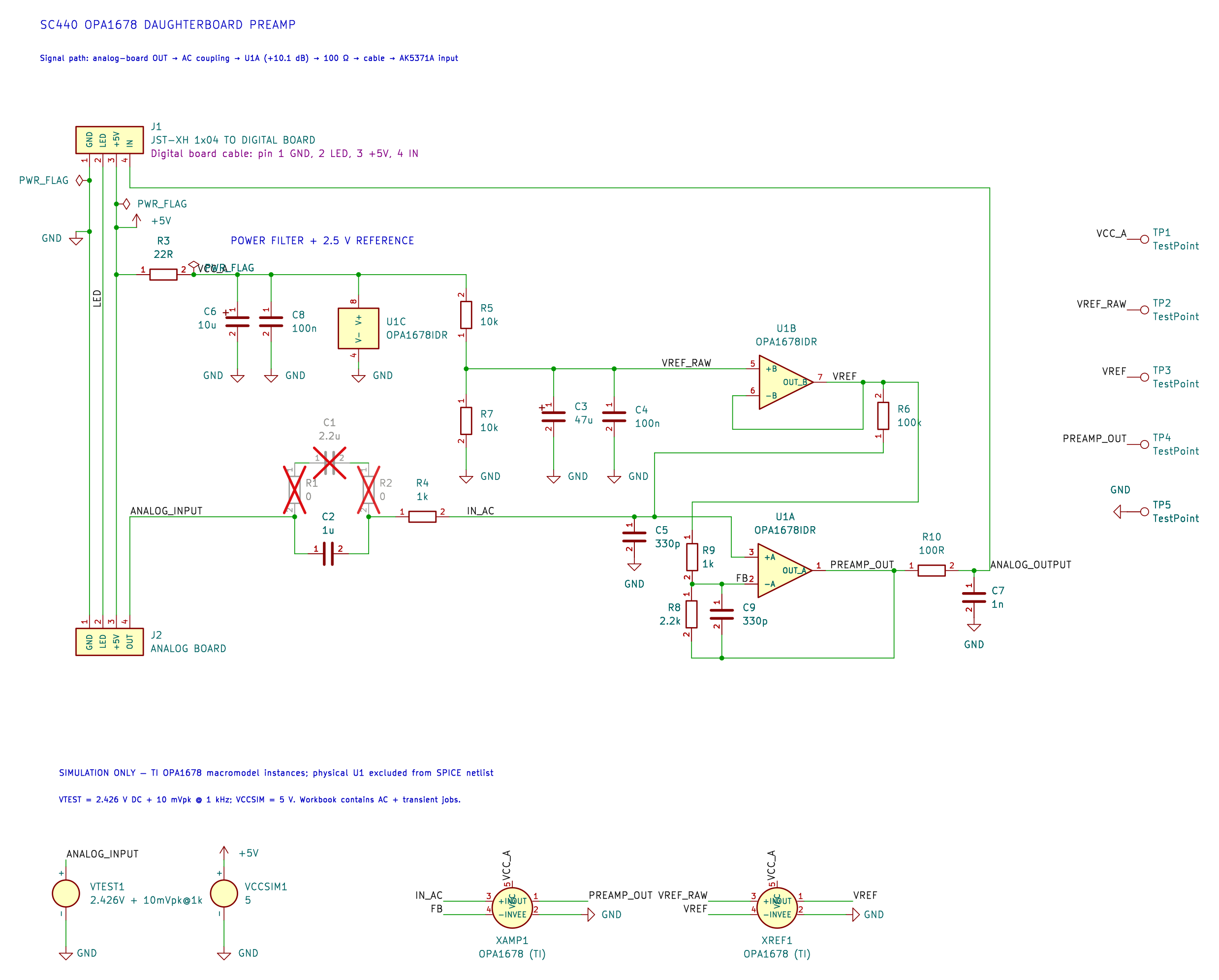
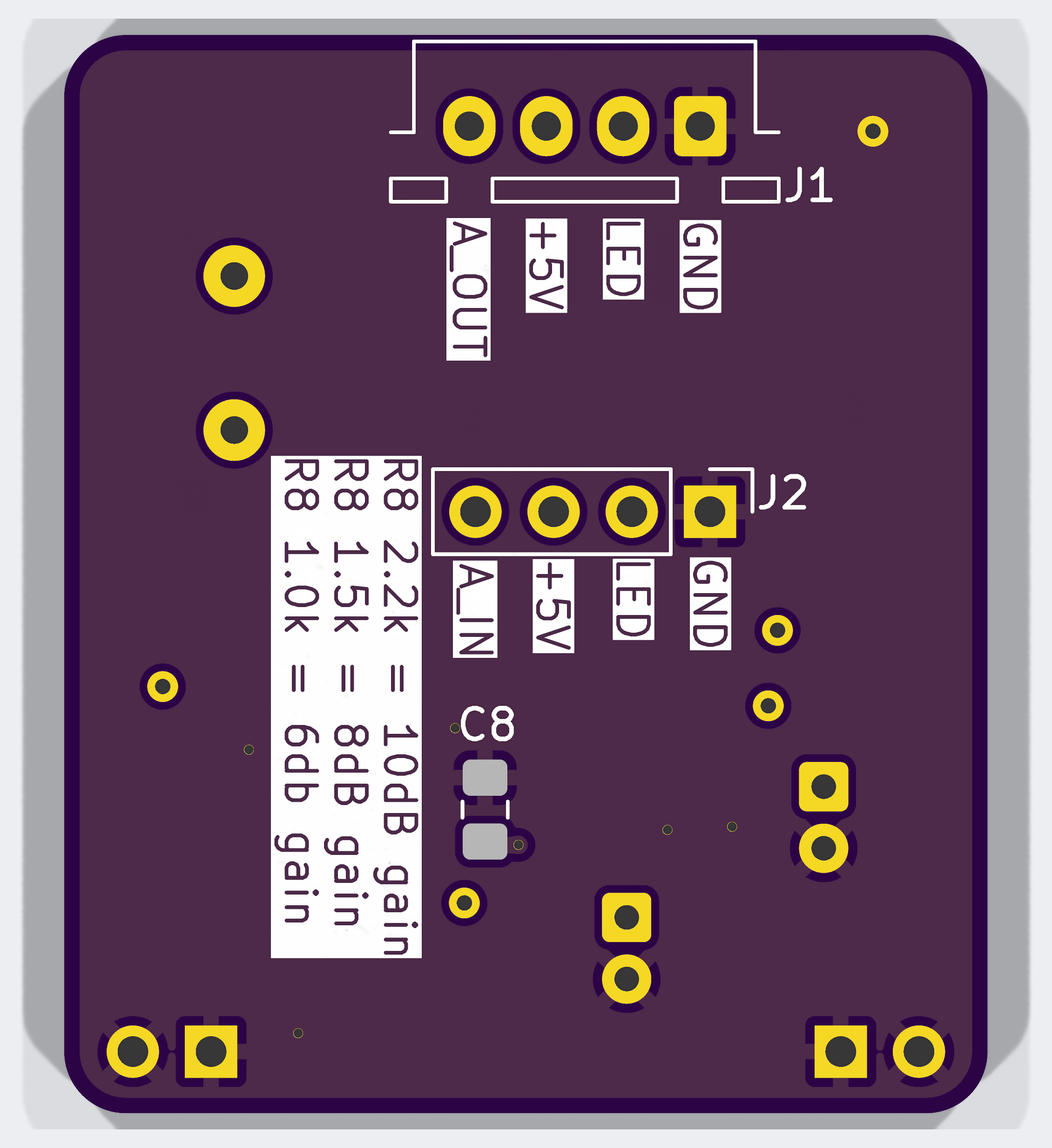
J1 is the digital-board connector; J2 is the analog-board connector. Both are installed on the back of this PCB. The two pitches differ: JST XH is 2.50 mm, the unshrouded analog header is 2.54 mm.
| Pin number | J2 — from analog board | J1 — to digital board | Connection on this PCB |
|---|---|---|---|
| 1 | GND | GND | Direct common ground |
| 2 | LED | LED | Direct pass-through |
| 3 | +5V | +5V | Direct pass-through; preamp supply branches through R3 |
| 4 | ANALOG_INPUT | ANALOG_OUTPUT | Through coupling capacitor, amplifier and R10; not direct |
Use pad numbers, including the square pin-1 pad, rather than assuming a left-to-right order from a photograph. Back-side placement and mirrored views change the apparent order. Check the cable at both ends before connecting USB.
The intended installation mounts the daughterboard behind the original analog PCB. Remove/reposition the original analog-board pin headers to the opposite side to make the required board-to-board connection. Replace the original digital-board pin socket with a JST XH header and use a short 4-wire cable to J1. Verify actual original-board holes, mating parts and enclosure clearance before final soldering; the daughterboard files do not define those original board footprints.
Keep the existing series DC-blocking capacitor on the digital-board audio input. J1 pin 4 carries the amplified AC signal on a DC level near VREF. There is no output coupling capacitor on the daughterboard itself. The microphone's exact ADC-side connection must be checked on the physical digital board.
C6 needs to be mounted lying down in the intended enclosure. Its CAD model is a generic upright radial capacitor, so the 3D view is not the final assembly orientation. Preserve polarity, avoid stressing the lead seals, and keep the body/metalwork clear of exposed conductors. Check C3 and the optional C1 against available height too. C1 currently has no attached 3D model.
| Block | Actual parts / connections | Purpose / approximate behavior |
|---|---|---|
| Supply filter | R3 = 22 Ω; C6 = 10 µF and C8 = 100 nF from VCC_A to GND | Filters raw USB 5 V; ideal R3/C6 pole ≈723 Hz |
| Reference divider | R5 = 10 kΩ from VCC_A to VREF_RAW; R7 = 10 kΩ to GND; C3 = 47 µF and C4 = 100 nF to GND | Approximately VCC_A/2; divider/C3 pole ≈0.68 Hz |
| Reference buffer | U1B: pin 5 at VREF_RAW, pins 6/7 at VREF | Low-impedance reference for input bias and feedback |
| Input coupling / bias | C2 or C1/R1/R2; R4 = 1 kΩ; R6 = 100 kΩ to VREF | Blocks original-board DC and establishes the amplifier bias |
| Input RF filter | R4 with C5 = 330 pF from IN_AC to GND | Pole approximately 0.48 MHz for a low-impedance source; source impedance also matters |
| Amplifier | U1A; R8 from PREAMP_OUT to FB, R9 from FB to VREF | Gain selected by R8/R9 |
| Feedback HF shaping | C9 = 330 pF parallel to R8 | Gradually reduces gain toward unity above the feedback pole |
| Output isolation / filter | R10 = 100 Ω; C7 = 1 nF from ANALOG_OUTPUT to GND | Isolates capacitive cable/input load; ideal RC pole ≈1.59 MHz |
These pole calculations describe individual networks, not the complete loaded frequency response. Cable/ADC loading and the op-amp's finite bandwidth also contribute. Do not add a large capacitor directly to the buffered VREF output without checking the buffer's capacitive-load stability; C3/C4 are on VREF_RAW.
| Test pad | Net | Expected DC with USB connected, no audio |
|---|---|---|
| TP1 | VCC_A | Raw +5V minus the drop across R3; at least 4.5 V for OPA1678 operation |
| TP2 | VREF_RAW | Approximately TP1/2 |
| TP3 | VREF | Approximately TP2 |
| TP4 | PREAMP_OUT | Approximately TP3 |
| TP5 | GND | Probe reference |
Raw USB voltage was reported above 4.9 V. At roughly 4.2 mA quiescent draw the 22 Ω resistor drops about 0.09 V; this is an estimate, not a minimum-voltage measurement at the IC. Check TP1 under operation. The input signal is centered near half supply; OPA1678 is not rail-to-rail at its inputs.
For commissioning, first check power and reference voltages, then compare recordings at equal final level with reduced ADC gain. Check clipping with loud speech/plosives and look for USB-related spurs. A valid rendering or simulated trace does not replace those measurements.
The included images represent the saved default assembly (10 dB, MLCC).
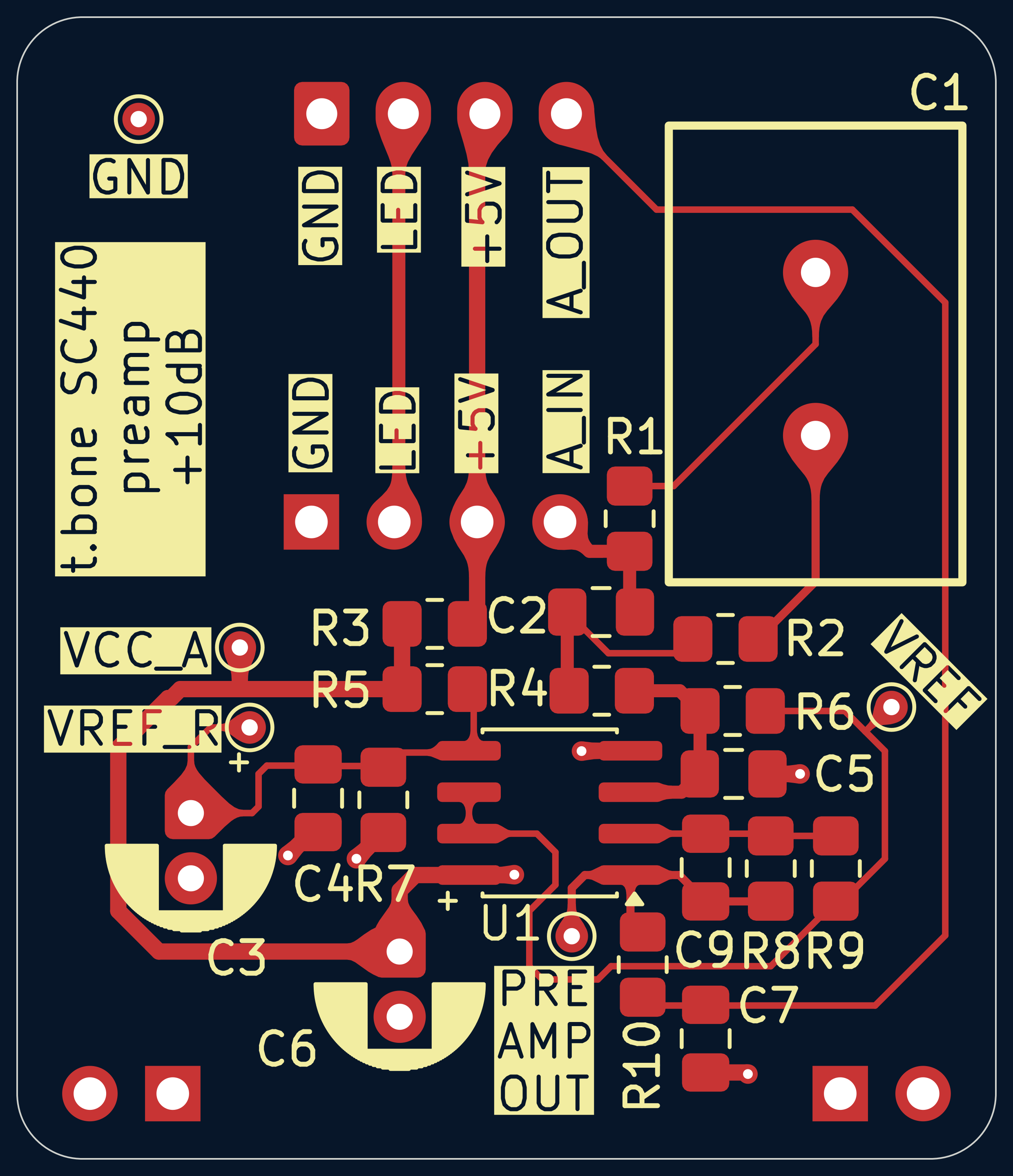
Copper, front silkscreen and board outline.
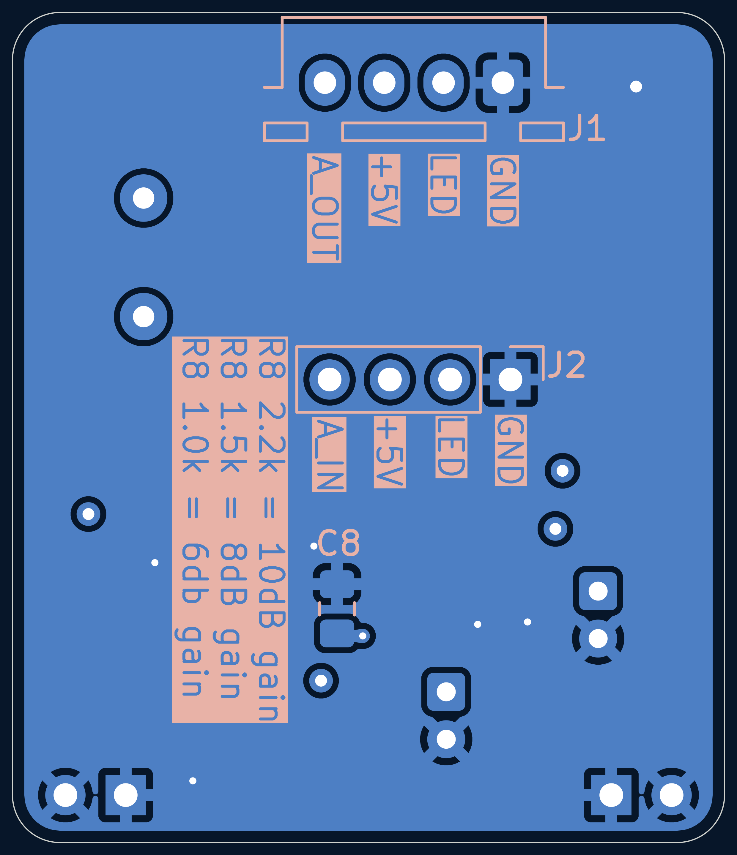
Rear copper/silkscreen and board outline, mirrored as viewed from the back.
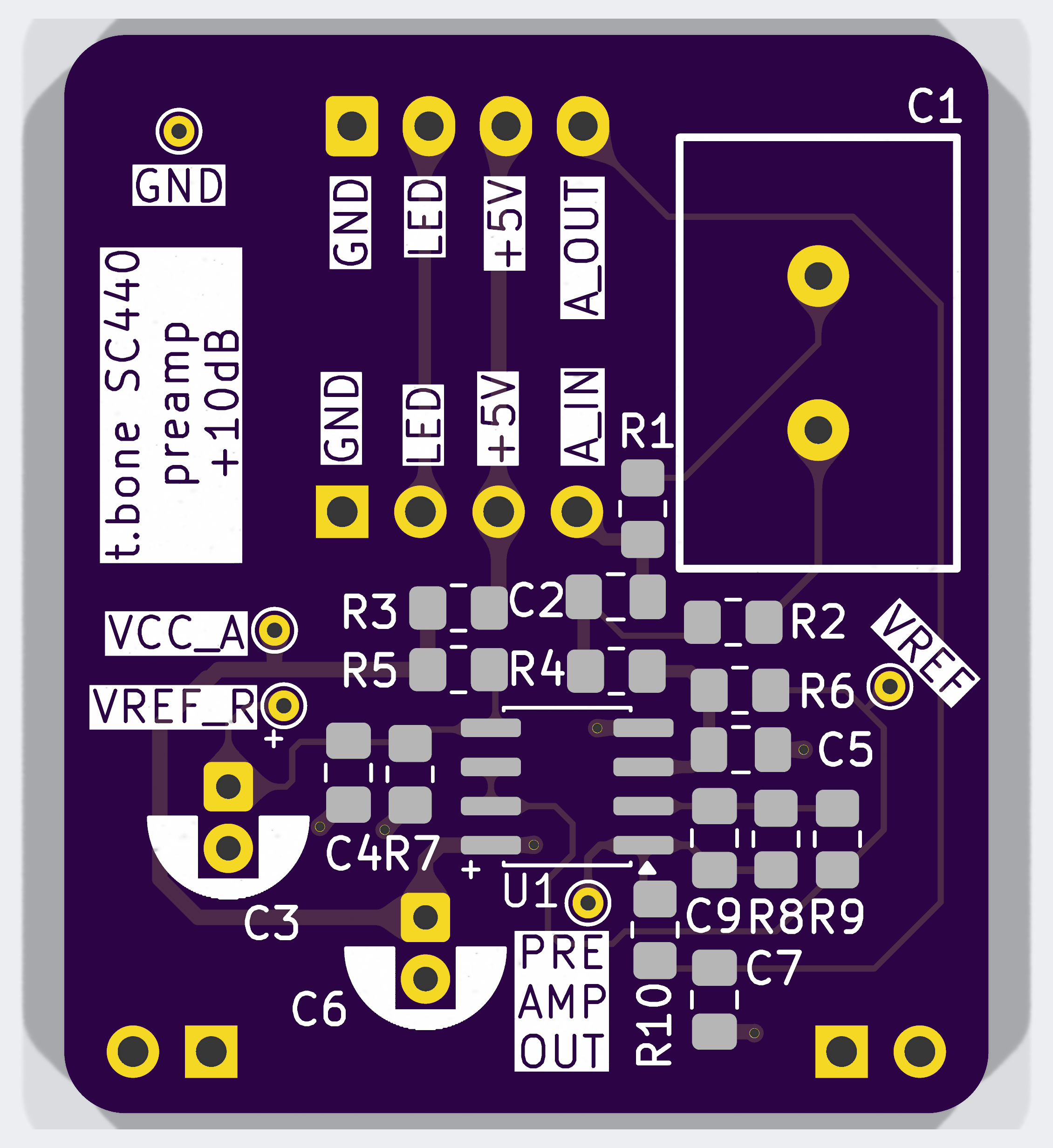
DNP models are omitted. C6's generic upright model and C1's missing model mean these images do not establish enclosure fit for every assembly variant.
There are two model paths. Both schematics and both reference netlists now use the current hardware topology and component references. The AC project was derived from the root schematic, with its AC-model properties, simulation annotations and project metadata adapted.
| File / project | Status in this revision | Appropriate use |
|---|---|---|
Root SC440_Preamp.kicad_sch + .wbk | Current root hardware values, including 2.2 kΩ/1 kΩ, R4/C5/C7/C9; default MLCC path | Transient / operating-point work after preparing the local TI model; not newly executed for this documentation update |
AC_SIM/SC440_Preamp_AC.kicad_sch + .wbk | Current root topology; self-contained AC model; workbook plots output gain/phase | Current unloaded small-signal response for the default 10 dB / MLCC assembly |
SC440_Preamp_fallback.cir | Current topology and references, including input/output filters and C9 | Transient fallback after preparing the TI model |
AC_SIM/SC440_Preamp_AC_reference.cir | Current topology and references | Standalone AC analysis using the included model |
The root schematic uses a local ngspice adaptation of TI's OPA167x TINA-TI Spice Model (SBOMAC5D). Download it from the TI OPA1678 product page, then run from the project root:
python3 tools/prepare_ti_model.py ~/Downloads/sbomac5d.zipThis creates vendor/OPA167x_ngspice.LIB. The TI model is not shipped here.
The converter recognizes the documented Final 1.6 source hash; syntax adaptation
does not guarantee compatibility with every KiCad/ngspice version. The modified
noise and protection cells are not vendor-accurate. Treat the prepared model as
a simulation aid, not proof of measured noise or protection performance.
The AC model is project-authored and self-contained, with typical 114 dB open-loop gain and 16 MHz GBW. It does not model clipping, slew, noise or rail limits. Both AC files default to 10 dB / MLCC; change their R8/input assembly when investigating other variants. Cable and ADC loading are not modeled. See SIMULATION_SPLIT.md and AC_SIM/README.md. All six assembly variants were run with ngspice 42 using the included AC model. Results and validation limits are in SIMULATION_VALIDATION.md. Model setup details are in SIMULATION_MODEL.md.
Save schematic and PCB changes in KiCad first. The generator reads the saved
files, refills zones in a temporary PCB copy, exports each PCB side separately,
and renders the 3D component sides with KiCad's top/bottom views.
Install Python, Pillow and Inkscape. From the project root:
python3 -m venv .venv
source .venv/bin/activate
python -m pip install Pillow
python tools/regenerate_readme_images.py \
  --kicad-cli "/Applications/KiCad-nightly-260925/KiCad.app/Contents/MacOS/kicad-cli" \
  --inkscape "/Applications/Inkscape.app/Contents/MacOS/inkscape"
Those app paths are the current macOS example; adjust them for your installation.
The script can discover common app/PATH locations automatically. Use
--models-dir PATH if the installed 3D library cannot be resolved. It normally
rejects missing model files; --allow-missing-models explicitly allows incomplete
renders. DNP footprints' models are omitted automatically.
No KiCad source file is rewritten by the image generator. Images are staged and
validated before replacement. The old combined PCB image reference, if present,
is converted to front/back references in README.md only after successful exports.
For more detail on PCB views, override --pcb-front-layers and
--pcb-back-layers; fabrication/courtyard layers are omitted by default to keep
these views readable.
Project-authored content is GPL-3.0-only, except where separately noted: LICENSE.md, LICENSES/GPL-3.0-only.txt. No TI SPICE macro-model is included or relicensed. See THIRD_PARTY_NOTICES.md and vendor/README.md.
| Qty | Value | Footprint | References |
|---|---|---|---|
| 5 | TestPoint | TestPoint:TestPoint_THTPad_D1.0mm_Drill0.5mm | TP1, TP2, TP3, TP4, TP5 |
| 2 | 0 | Resistor_SMD:R_0805_2012Metric_Pad1.20x1.40mm_HandSolder | R1, R2 |
| 2 | 100n | Capacitor_SMD:C_0805_2012Metric_Pad1.18x1.45mm_HandSolder | C4, C8 |
| 2 | 10k | Resistor_SMD:R_0805_2012Metric_Pad1.20x1.40mm_HandSolder | R5, R7 |
| 2 | 1k | Resistor_SMD:R_0805_2012Metric_Pad1.20x1.40mm_HandSolder | R4, R9 |
| 2 | 330p | Capacitor_SMD:C_0805_2012Metric_Pad1.18x1.45mm_HandSolder | C5, C9 |
| 1 | 100R | Resistor_SMD:R_0805_2012Metric_Pad1.20x1.40mm_HandSolder | R10 |
| 1 | 100k | Resistor_SMD:R_0805_2012Metric_Pad1.20x1.40mm_HandSolder | R6 |
| 1 | 10u | Capacitor_THT:CP_Radial_D5.0mm_P2.00mm | C6 |
| 1 | 1n | Capacitor_SMD:C_0805_2012Metric_Pad1.18x1.45mm_HandSolder | C7 |
| 1 | 1u | Capacitor_SMD:C_0805_2012Metric_Pad1.18x1.45mm_HandSolder | C2 |
| 1 | 2.2k | Resistor_SMD:R_0805_2012Metric_Pad1.20x1.40mm_HandSolder | R8 |
| 1 | 2.2u | SC440_Preamp:Faratronic_C241J225_P5.00mm | C1 |
| 1 | 22R | Resistor_SMD:R_0805_2012Metric_Pad1.20x1.40mm_HandSolder | R3 |
| 1 | 47u | Capacitor_THT:CP_Radial_D5.0mm_P2.00mm | C3 |
| 1 | ANALOG BOARD | Connector_PinHeader_2.54mm:PinHeader_1x04_P2.54mm_Vertical | J2 |
| 1 | JST-XH 1x04 TO DIGITAL BOARD | Connector_JST:JST_XH_B4B-XH-A_1x04_P2.50mm_Vertical | J1 |
| 1 | OPA1678IDR | Package_SO:SOIC-8_3.9x4.9mm_P1.27mm | U1 |
The 27 most common of 29 parts.


Loredati-svg/TPA3116D2-Class-D-Amplifier
2×50W stereo Class-D audio amplifier based on TI TPA3116D2 – KiCad PCB design


dmsd-lab/AMP8611
AMP8611 - open hardware integrated stereo power amplifier with a 2-channel input selector, PGA2311 digital volume control and LM3886 power stages

GasimovDev/guitar-pedal
A digital guitar pedal. Guitar in, an STM32 microcontroller runs three effects (overdrive, then tremolo, then delay), and the sound comes out to your amp. It has six knobs, three footswitches and three LEDs.

tieziyun/ultrasonic-aesa
A 40 kHz in-air phased array, an acoustic "AESA". It has 64 transducers in an 8 × 8 grid, and each one can transmit or listen under FPGA control, element by element and ping by ping.

misko/prompt2device
The separate vNext PCB skill and orchestrator package is available alongside the reference workflow below; existing projects keep their accepted toolchain until an explicit migration.
It measures 30 × 35 mm and has 2 copper layers, 1.6 mm thick.
29 parts, built around the OPA1678IDRGR. The full list of its parts is on this page, with links to each part's symbol and footprint where PCBKit's library has them.
From the lk-ek/SC440_Preamp repository on GitHub, at the commit this page was made from: the board is SC440_Preamp.kicad_pcb and its schematic AC_SIM/SC440_Preamp_AC.kicad_sch. PCBKit opens the board in the browser, with nothing to install.
Its repository states no licence, so its author keeps all rights: ask lk-ek before reusing the design.