
2 layers85.4 × 54.1 mm

 linux4life798/business-card
My personal and extensible PCB business card with NFC.
Business card is an open-source printed circuit board by linux4life798, from the linux4life798/business-card repository on GitHub, published under the MIT licence. It is a 2-layer board of 85.6 × 54 mm with 15 parts on 9 nets, routed with 89 tracks and 12 vias.
It is built around the NT3H2111W0FHKH and A-SP192SS1C-C01-3C. Its parts include 4 resistors, 3 capacitors, 1 IC, 1 diode and 1 connector. It belongs with the radio and wireless boards of this library.
A thin, wallet-size PCB business card combining printed contact details, a vCard QR code, custom copper and silkscreen artwork, and passive NFC.
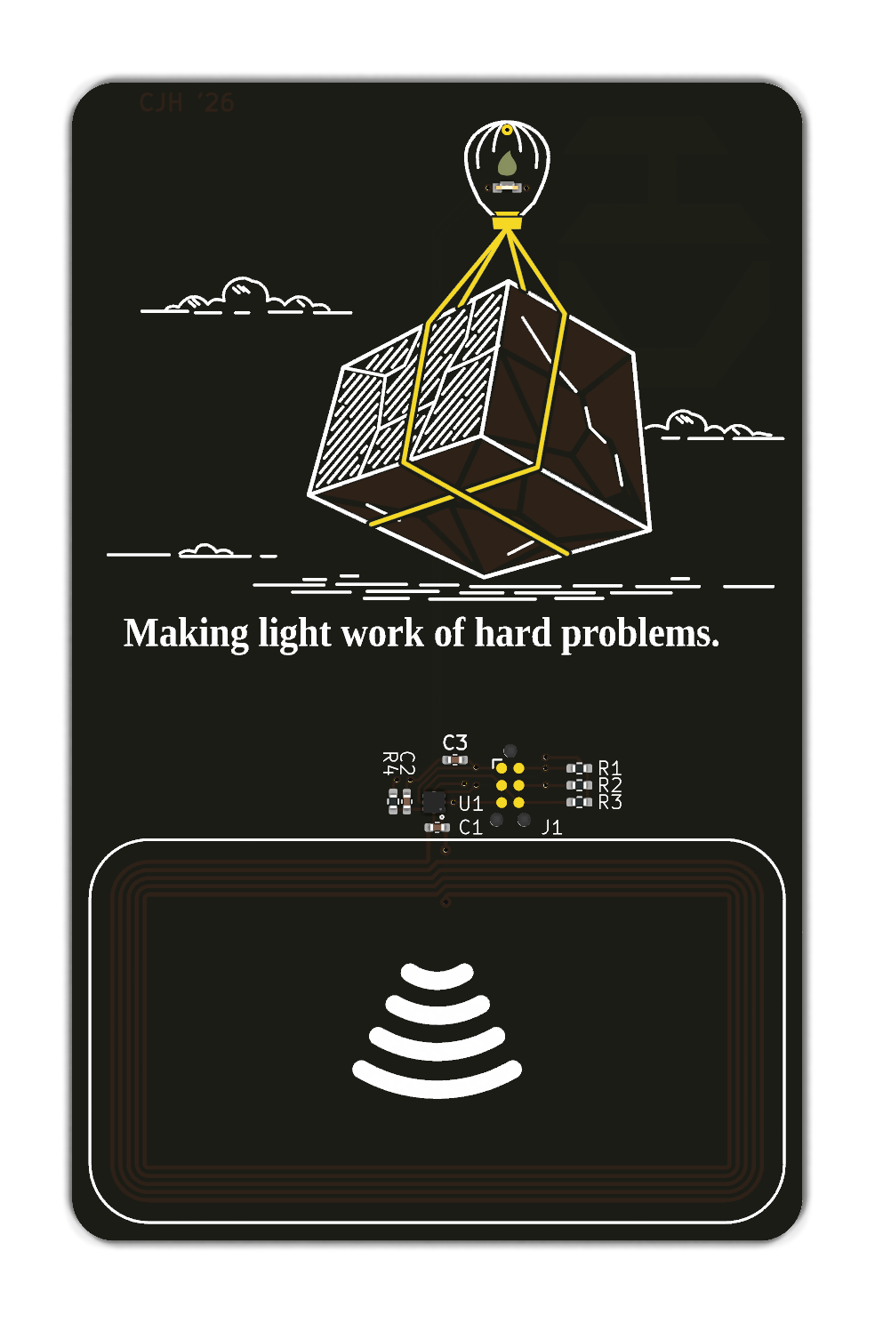
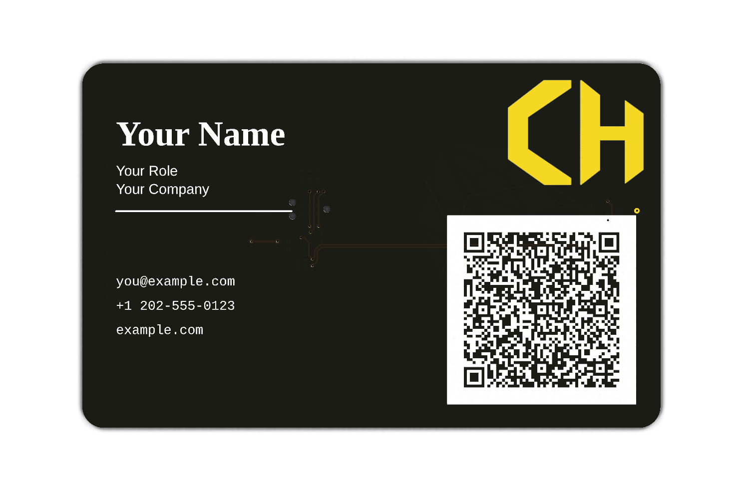
KiCad 3D renders of the front and back, with gold on exposed copper.
You can personalize and export the card entirely through KiCad 10. Python and GitHub Actions are optional conveniences.
CONTACT_* fields.
Company, role, phone, email and website are optional. CONTACT_WEB is the
printed address; CONTACT_WEB_QR is the QR's full URL, including https://.The finalizer creates a personalized project copy and export
bundle. It uses the saved INFO1 values; to override them only in the exported
copy, copy contact.example.toml to contact.toml and edit
it. Omitted keys keep the INFO1 value; "" clears an optional field. For CI,
CONTACT_* environment variables override both TOML and INFO1, including empty values.
Use Python 3.11+ with KiCad 10's kicad-cli on your PATH and standard 3D model
libraries installed. No pip packages or virtual environment are needed:
python3 copy-and-customize.py
python3 copy-and-customize.py --config contact.personal.toml --output output/personal
On Windows, use python instead of python3. The KiCad 10 Command Prompt
provides access to kicad-cli.
The bundle contains a project-folder copy, Gerbers/drills and drill-map PDFs in
fab/, refreshed schematic SVG/PDF and front/back renders in docs/, and drc.rpt.
Local settings, contact files, caches and previous exports are excluded.
It defaults to output/<timestamp>/ plus one ZIP, preserving source files and
existing exports. Review the report and previews before ordering; DRC findings
do not prevent export. The exported project remains editable through the same
INFO1 workflow; regenerate fabrication files after further edits.
For builds on GitHub, see the private-repository action and starter workflow.
The NFC circuit uses an NXP NT3H2111W0FHKH (NTAG I2C Plus) and a printed antenna. It is designed to illuminate an LED using energy from the reader's field, with no onboard battery or microcontroller.
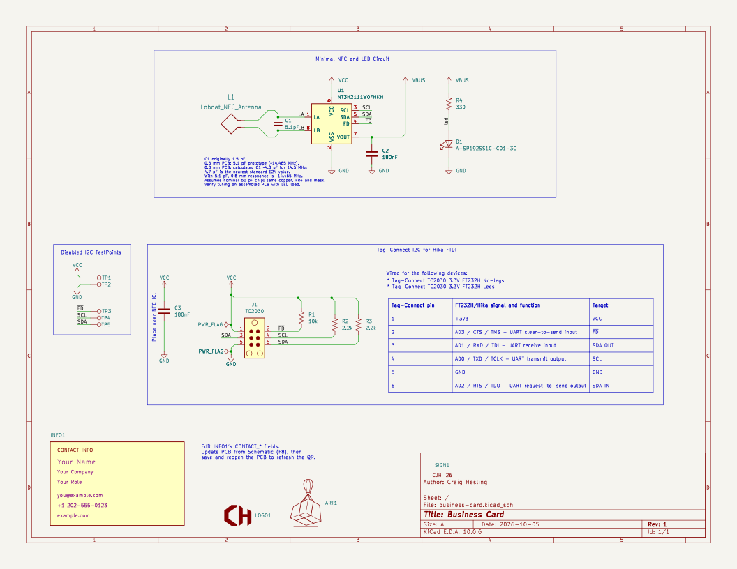
INFO1 supplies the fields used by the contact-info footprint for its text and native QR. If a footprint library update restores default contact values, repeat F8 and the save/reopen step to reapply your details.
Fabrication targets a two-layer, 0.6 mm FR-4 board with 1 oz copper, black solder mask, and lead-free HASL.
Antenna tuning, NFC read range, and LED brightness require validation on assembled hardware.
| Qty | Value | Footprint | References |
|---|---|---|---|
| 2 | 180nF | Capacitor_SMD:C_0402_1005Metric_Pad0.74x0.62mm_HandSolder | C2, C3 |
| 2 | 2.2k | Resistor_SMD:R_0402_1005Metric_Pad0.72x0.64mm_HandSolder | R2, R3 |
| 1 | 10k | Resistor_SMD:R_0402_1005Metric_Pad0.72x0.64mm_HandSolder | R1 |
| 1 | 330 | Resistor_SMD:R_0402_1005Metric_Pad0.72x0.64mm_HandSolder | R4 |
| 1 | 5.1pF | Capacitor_SMD:C_0402_1005Metric_Pad0.74x0.62mm_HandSolder | C1 |
| 1 | A-SP192SS1C-C01-3C | business-card:Amicc_A-SP192SS1C-C01-3C_SideView | D1 |
| 1 | CH_Logo | business-card:CH_Logo_20mm_Copper | LOGO1 |
| 1 | CJH_Signature | business-card:CJH_Signature_Copper_Masked | SIGN1 |
| 1 | Contact_Info | business-card:Contact_Info_SilkScreen | INFO1 |
| 1 | LanternLift_GiftWrap | business-card:LanternLift_GiftWrap_Copper_SilkScreen | ART1 |
| 1 | Loboat_NFC_Antenna | business-card:Loboat_NFC_Antenna_48x25mm_5Turns | L1 |
| 1 | NT3H2111W0FHKH | business-card:NXP_SOT902-3_XQFN-8_1.6x1.6mm | U1 |
| 1 | TC2030 | Connector:Tag-Connect_TC2030-IDC-NL_2x03_P1.27mm_Vertical | J1 |


nushackers/hnr26-badge-quacknroll
Hack&Roll 2026 "Quack & Roll" badge source files, for both hardware and firmware


ElectronicCats/badge-dragonJar-2025
¡El badge oficial de DragonJarCON 2025! Un dispositivo NFC programable con pantalla OLED, múltiples LEDs y un reto de hacking integrado. Diseñado para la comunidad de DragonJar


It measures 85.6 × 54 mm and has 2 copper layers, 0.6 mm thick.
15 parts, built around the NT3H2111W0FHKH and A-SP192SS1C-C01-3C. The full list of its parts is on this page, with links to each part's symbol and footprint where PCBKit's library has them.
From the linux4life798/business-card repository on GitHub, at the commit this page was made from: the board is business-card.kicad_pcb and its schematic business-card.kicad_sch. PCBKit opens the board in the browser, with nothing to install.
Its repository publishes it under the MIT licence: you may reuse it on that licence's terms (keep the author's notice, and for a copyleft licence share your changes alike).