2 layers66 × 48 mm
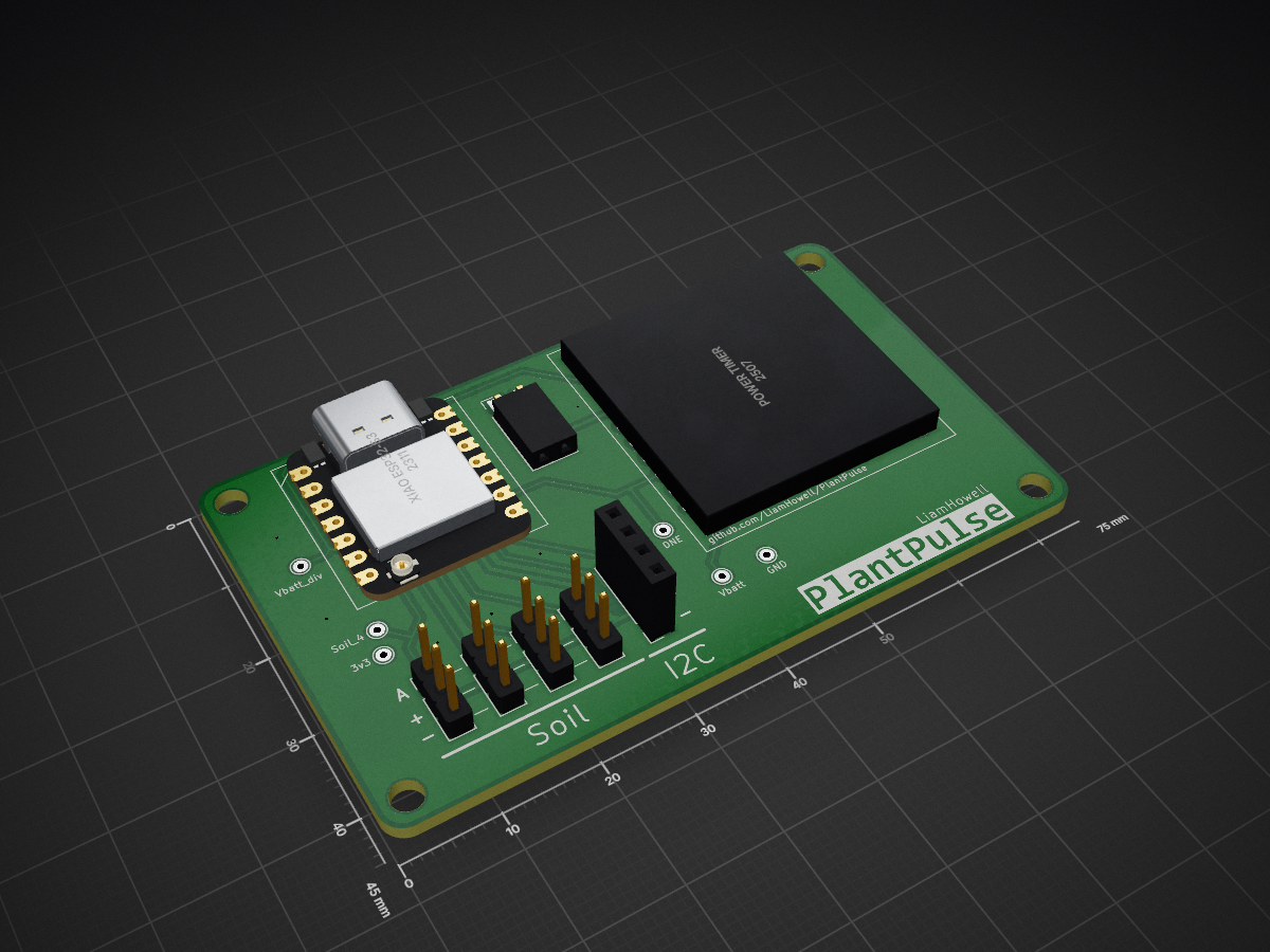
 LiamHowell/PlantPulse---Node---PCB
PlantPulse Node is an open-source printed circuit board by LiamHowell, from the LiamHowell/PlantPulse---Node---PCB repository on GitHub, published under the MIT licence. It is a 2-layer board of 75 × 45 mm with 21 parts on 18 nets, routed with 94 tracks and 13 vias.
Its parts include 6 connectors, 2 resistors and 2 ICs. It belongs with the ESP32 boards of this library.
| Qty | Value | Footprint | References |
|---|---|---|---|
| 2 | 10k | Resistor_THT:R_Axial_DIN0207_L6.3mm_D2.5mm_P7.62mm_Horizontal | R1, R2 |
| 1 | 3v3 | TestPoint:TestPoint_THTPad_D1.5mm_Drill0.7mm | TP6 |
| 1 | DNE | TestPoint:TestPoint_THTPad_D1.5mm_Drill0.7mm | TP4 |
| 1 | GND | TestPoint:TestPoint_THTPad_D1.5mm_Drill0.7mm | TP5 |
| 1 | I2C_Port | Connector_PinSocket_2.54mm:PinSocket_1x04_P2.54mm_Vertical | J6 |
| 1 | LOGO | Footprints-General:plantpulse-artwork | G*** |
| 1 | Power Timer | Footprints-General:Nano Power Timer | U2 |
| 1 | Soil_4 | TestPoint:TestPoint_THTPad_D1.5mm_Drill0.7mm | TP7 |
| 1 | Soil_Sensor1 | Connector_PinHeader_2.54mm:PinHeader_1x03_P2.54mm_Vertical | J2 |
| 1 | Soil_Sensor2 | Connector_PinHeader_2.54mm:PinHeader_1x03_P2.54mm_Vertical | J3 |
| 1 | Soil_Sensor3 | Connector_PinHeader_2.54mm:PinHeader_1x03_P2.54mm_Vertical | J4 |
| 1 | Soil_Sensor4 | Connector_PinHeader_2.54mm:PinHeader_1x03_P2.54mm_Vertical | J5 |
| 1 | Vbatt | TestPoint:TestPoint_THTPad_D1.5mm_Drill0.7mm | TP1 |
| 1 | Vbatt_div | TestPoint:TestPoint_THTPad_D1.5mm_Drill0.7mm | TP2 |
| 1 | Xiao ESP32-S3 | Footprints-General:Xiao-S3 | U1 |
| 1 | Xiao_Batt_Conn | Connector_PinSocket_2.54mm:PinSocket_1x02_P2.54mm_Horizontal | J1 |
The 17 most common of 21 parts.

gusmanb/logicanalyzer
24 channel, 100Msps logic analyzer hardware and software

mntmn/amiga2000-gfxcard
MNT VA2000, an Open Source Amiga 2/3/4000 Graphics Card (Zorro II/III), written in Verilog


hackclub/OnBoard
💡 Join 1,000 teenagers and make your first PCB with a $100 grant!

drandyhaas/KiCadRoutingTools
A set of Python/Rust tools to aid routing in KiCad

Arrow-air/project-quiver
Project Quiver documentation, designs, and project artifacts.


It measures 75 × 45 mm and has 2 copper layers, 1.6 mm thick.
21 parts. The full list of its parts is on this page, with links to each part's symbol and footprint where PCBKit's library has them.
From the LiamHowell/PlantPulse---Node---PCB repository on GitHub, at the commit this page was made from: the board is Node V20/PlantPulse_Node.kicad_pcb and its schematic Node V10/Node V10.kicad_sch. PCBKit opens the board in the browser, with nothing to install.
Its repository publishes it under the MIT licence: you may reuse it on that licence's terms (keep the author's notice, and for a copyleft licence share your changes alike).