2 layers40 × 30 mm

 lgili/Fenolite1
PCB automation in Python, for engineers and AI agents.
Channel is an open-source printed circuit board by lgili, from the lgili/Fenolite repository on GitHub, published under the Apache-2.0 licence. It is a 2-layer board of 16 × 8 mm with 3 parts on 3 nets, routed with 6 tracks and 0 vias.
Its parts include 1 capacitor, 1 resistor and 1 diode.
PCB automation in Python, for engineers and AI agents.
Create PCB projects from code, inspect KiCad and Altium files, and review designs in your browser. Use the Python library or a CLI with structured JSON results, explicit write plans and conversion loss reports.


Get started · Documentation · Examples · What's in 0.5 · Get help
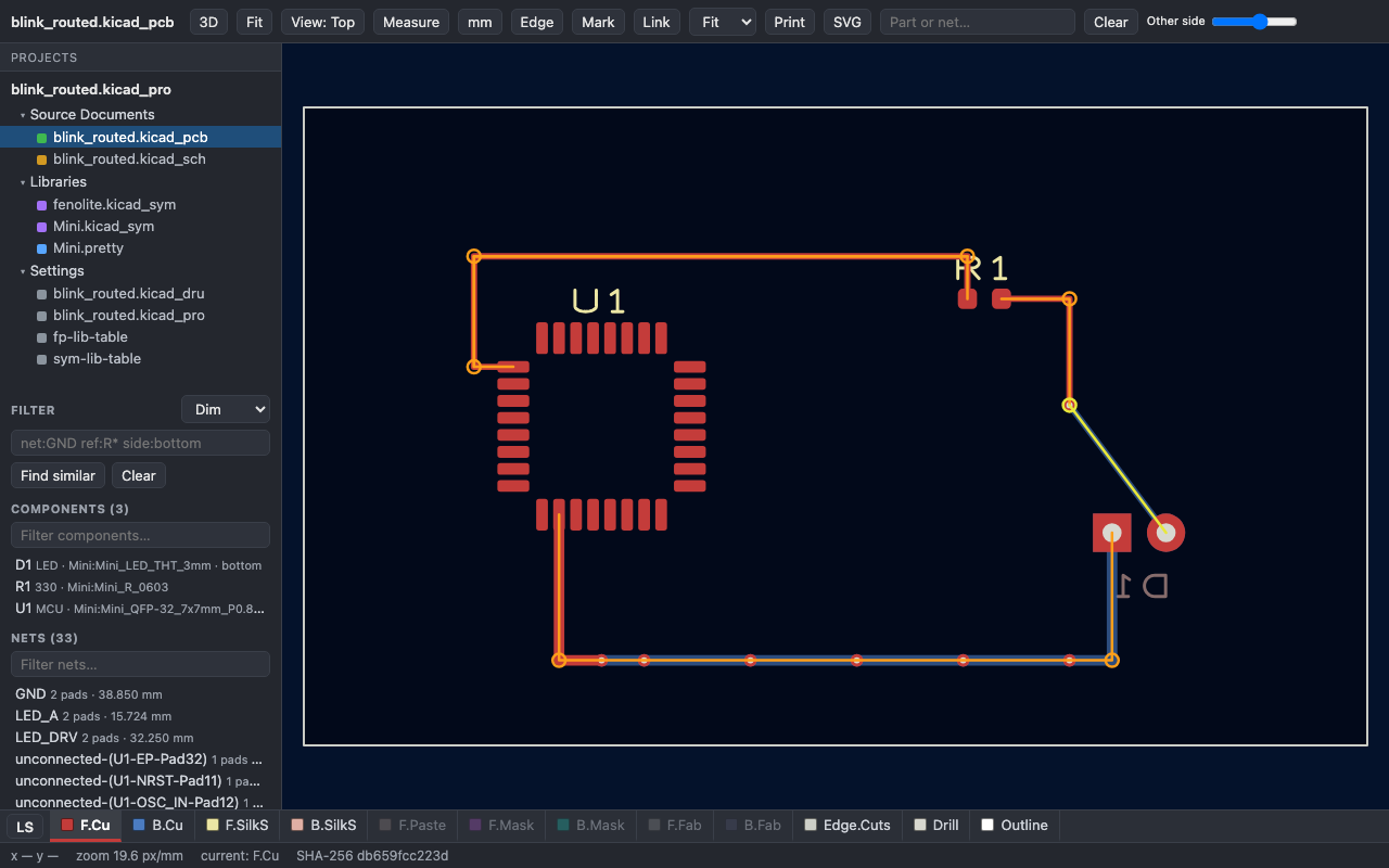
Actual Fenolite viewer, using a small example authored for this project. No KiCad or Altium installation is needed to view it.
Requires Python 3.11+. It installs no other package. Heavier features are optional extras.
python -m pip install fenolite
fenolite capabilities --brief --json
fenolite init blink --confirm --json
fenolite build blink/design.py --out blink/build --confirm --json
fenolite view blink/build --serve
Open the local address printed by the viewer. You now have a PCB and a schematic built from
blink/design.py, using the built-in component catalog. No external CAD libraries are needed.
These commands create a new blink folder; use a fresh location.
This starter is a header, resistor and LED. It is an educational example; choose parts, ratings, placement and rules for your own circuit before manufacturing. For reviewed write plans, a standalone HTML export and routing, follow the quickstart.
Open a KiCad or Altium project, board, schematic or library. Explore layers, highlight nets, measure geometry and navigate between documents. Export a standalone HTML page for review.
fenolite view board.kicad_pcb --serve
fenolite view Project.PrjPcb --export review.html --confirm --json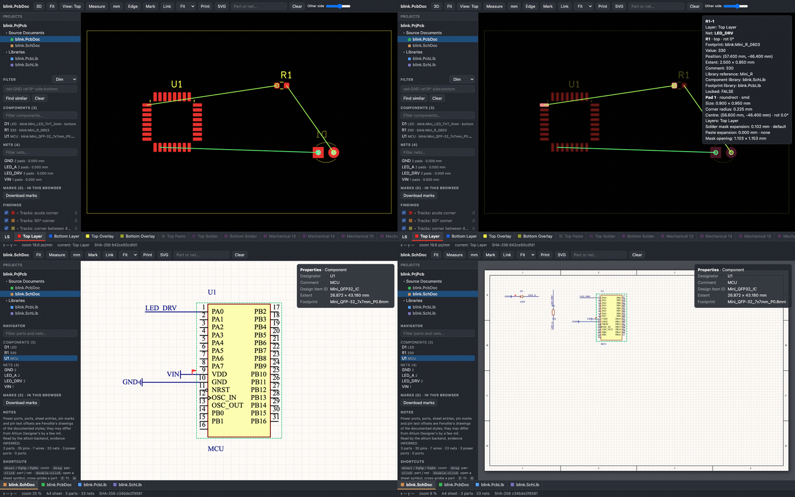
The animation uses Fenolite's authored Altium Blink fixture. See the viewer guide for supported items, 3D prerequisites and rendering limits.
Define components, connections, placement and copper in a versioned source file. Build a project that can also be opened in its CAD editor. Preserve board edits on rebuild and sync placements back to source.
from fenolite.dsl import Design, Net, Part, connect, mm

design = Design("led")
design.board(mm(30), mm(20))
r1 = Part("R1", "Fenolite:Resistor", footprint="Fenolite:Chip_0603", value="330")
d1 = Part("D1", "Fenolite:LED", footprint="Fenolite:Chip_0603", value="LED")
design.add(r1, d1)
connect(Net("LED_A"), r1[2], d1[1])
r1.place(mm(10), mm(10))
d1.place(mm(20), mm(10))
This small fragment illustrates the DSL, not a complete powered circuit. Start with the complete starter tutorial, then explore authored examples and the Python DSL.
KiCad's CLI provides ERC, DRC, zone fills and fabrication exports. Production routing uses an external
router or copper declared in the script. The built-in direct router is for simple demonstrations.
Convert between KiCad and Altium, or write a KiCad 10 project for KiCad 9. Review what was kept, changed or lost, with a readback comparison against the source.
fenolite convert board.PcbDoc --to kicad --out converted --dry-run --json
fenolite equivalent before.kicad_pcb after.kicad_pcb --level 5 --json
Conversions and Altium writes are experimental in 0.7. Lossy conversion requires explicit consent. Support depends on the constructs in the input; review the report and the resulting design. Read the conversion guide.
The same commands return structured JSON, typed errors, evidence labels and file receipts.
A write can be previewed with --dry-run, then confirmed using its --plan identifier.
fenolite guide start --text
fenolite skill install --help
The package includes an agent guide and board-design practice pages. Agents can inspect parts, query nets and geometry, build, route, check and export using the same CLI as an engineer. See the agent guide and CLI contract.
Use a fresh folder for this complete loop. The first six lines need no external CAD tool; fill, check, export and render require KiCad's CLI. The direct router is a demonstration router.
fenolite capabilities --brief --json
fenolite init blink --confirm --json
fenolite build blink/design.py --out blink/build --dry-run --json
fenolite build blink/design.py --out blink/build --confirm --json
fenolite place blink/build --strategy grid --confirm --json
fenolite route blink/build --router direct --confirm --json
fenolite fill blink/build --confirm --json
fenolite check blink/build --json
fenolite export blink/build -o blink/fab --all --manifest --confirm --json
fenolite render blink/build -o blink/views --svg --png --confirm --json
For fabrication exports, BOM and placement tables, see exports and assembly.
Status: version 0.7. Python scripts build KiCad 9/10 PCB and schematic projects. The agent loop uses KiCad's ERC/DRC checks, the board engineering analyses and an MCP server; conversion supports KiCad/Altium and the older KiCad major. Altium writes, computed Altium pours and conversions are experimental. See the release scope and limits.
| Workflow | What you need | Status in 0.7 |
|---|---|---|
| Build the starter; inspect and view supported files | Python 3.11+, browser for the viewer | Shipped; format-specific rendering limits apply |
| KiCad project generation | Python; KiCad 9 or 10 to open in the editor | Shipped |
| KiCad ERC, DRC, fill and fabrication export | kicad-cli 9 or 10 | Shipped; engineering review still required |
| External routing | A supported router and its prerequisites | Freerouting and KiCadRoutingTools integrations |
| KiCad/Altium conversion and KiCad downgrade | Requirements vary by direction | Experimental; explicit loss report |
| Altium project generation | Python; Altium for native validation | Experimental |
Linux, macOS and Windows are supported. Optional extras include geo for polygon operations
and kicad-ipc for a live KiCad session. Since 0.6 the package includes the stdlib-only MCP server
(fenolite mcp), script editing and image replies described in the
MCP documentation. See
installation and prerequisites.
The viewer, conversion, board panels, slots and review tools ship since 0.5; 0.6 adds the MCP server, the board engineering tools (analyses, tidy, reuse, silkscreen, test points, DRC gates) and the Python API. 0.7 carries Altium boards through KiCad and back (rules, classes, planes, unions, fonts, computed pours), still experimental. Native Draftsman writing and Embedded Board Arrays remain gated. Detailed scope and deferred checks are in the release record.
Trying Fenolite on a public or self-authored example? Tell us what worked and where you got stuck. Ask a question or report a bug, including the version, command and error output. Keep private designs and personal paths out of public reports.
For development, clone the repository, run uv sync --extra dev
and read CONTRIBUTING.md.
Apache-2.0. Format knowledge comes from public sources under the project's clean-room rules. Results carry evidence labels; detailed claims live in the evidence matrix.
Fenolite is Portuguese for phenolic board material, the laminate many of us etched our first boards on.
| Qty | Value | Footprint | References |
|---|---|---|---|
| 1 | 100n | Fenolite:Chip_0805 | C1 |
| 1 | 1k | Fenolite:Chip_0603 | R1 |
| 1 | green | Fenolite:LED0603_Kingbright_APT1608SURCK | D1 |

hzeller/rpi-rgb-led-matrix
Controlling up to three chains of 64x64, 32x32, 16x32 or similar RGB LED displays using Raspberry Pi GPIO


atopile/atopile
Design circuit boards with code! ✨ Get software-like design reuse 🚀, validation, version control and collaboration in hardware; starting with electronics ⚡️


hackclub/sprig
🍃 Learn to code by making games in a JavaScript web-based game editor.
It measures 16 × 8 mm and has 2 copper layers, 1.6 mm thick.
3 parts. The full list of its parts is on this page, with links to each part's symbol and footprint where PCBKit's library has them.
From the lgili/Fenolite repository on GitHub, at the commit this page was made from: the board is examples/relative/channel.kicad_pcb. PCBKit opens the board in the browser, with nothing to install.
Its repository publishes it under the Apache-2.0 licence: you may reuse it on that licence's terms (keep the author's notice, and for a copyleft licence share your changes alike).