2 layers24.4 × 24.4 mm
OSO SWAT B1
joeycastillo/Sensor-Watch
A board replacement for the classic Casio F-91W wristwatch
39 parts2.1k
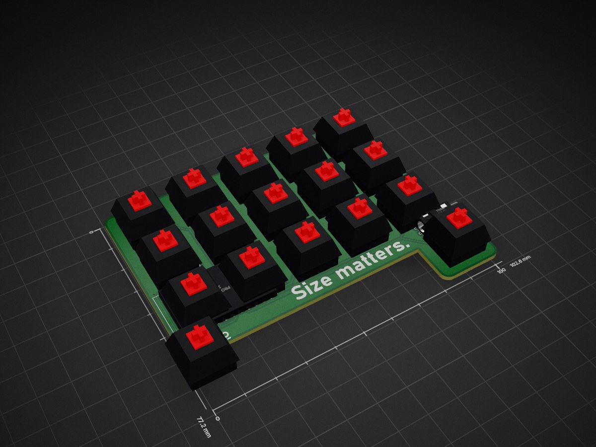
 lfgberg/splitty
pain27 esque ortho split
Splitty is an open-source printed circuit board by lfgberg, from the lfgberg/splitty repository on GitHub. It is a 2-layer board of 102.6 × 77.2 mm with 39 parts on 39 nets, routed with 229 tracks and 2 vias.
Its parts include 16 diodes and 2 ICs. It belongs with the AVR (ATmega, ATtiny) boards of this library.
pain27 esque ortho split
| Qty | Value | Footprint | References |
|---|---|---|---|
| 16 | D_Small | Footprints:Diode-dual | D1, D2, D3, D4, D5, D6, D7, D8, D9, D10, D11, D12, D13, D14, D15, D16 |
| 16 | MX-NoLED | Footprints:reversible-mx-alps-choc | MX1, MX2, MX3, MX4, MX5, MX6, MX7, MX8, MX9, MX10, MX11, MX12, MX13, MX14, MX15, MX16 |
| 2 | LOGO | Footprints:3.7x3.7mm-lg-silk | G***, G*** |
| 2 | LOGO | Footprints:size-matters-silk | G***, G*** |
| 1 | Jumper | Footprints:splitty-reset-jumper | JP1 |
| 1 | ProMicro | Footprints:splitty-pro-micro | U1 |
| 1 | TRRS | Footprints:TRRS_JACK_MJ4PP9 | U2 |
It measures 102.6 × 77.2 mm and has 2 copper layers, 1.6 mm thick.
39 parts. The full list of its parts is on this page, with links to each part's symbol and footprint where PCBKit's library has them.
From the lfgberg/splitty repository on GitHub, at the commit this page was made from: the board is KiCad/splitty/splitty.kicad_pcb. PCBKit opens the board in the browser, with nothing to install.
Its repository states no licence, so its author keeps all rights: ask lfgberg before reusing the design.
joeycastillo/Sensor-Watch
A board replacement for the classic Casio F-91W wristwatch

rusefi/rusefi
rusefi - GPL internal combustion engine control unit

hackclub/OnBoard
💡 Join 1,000 teenagers and make your first PCB with a $100 grant!

ataradov/usb-sniffer-lite
A simple USB sniffer based on Raspberry Pi RP2040

windowsair/wireless-esp8266-dap
CMSIS-DAP compatible wireless debugger for ESP8266/ESP32/ESP32C3/ESP32S3. Optional 40MHz SPI acceleration, etc. 适配多种ESP芯片的无线调试器


lachlanA/eagle-to-kicad
Eagle SCH/LIB to KiCad SCH/LIB ULP conversion script
