4 layers40 × 23 mm

 leoheck/beryl-breakout1
[WIP] Simple breakout board for GAPH's Beryl MBLite IC
Beryl breakout is an open-source printed circuit board by leoheck, from the leoheck/beryl-breakout repository on GitHub. It is a 4-layer board of 90 × 80 mm with 37 parts on 161 nets, routed with 105 tracks and 23 vias.
Its parts include 25 capacitors, 7 connectors and 1 IC. It belongs with the interfaces and adapters boards of this library.
Beryl Breakout Board
Simple, breakout for the huge IC made in the past. This is still a work in progress.
This project uses Kicad 5.6.1
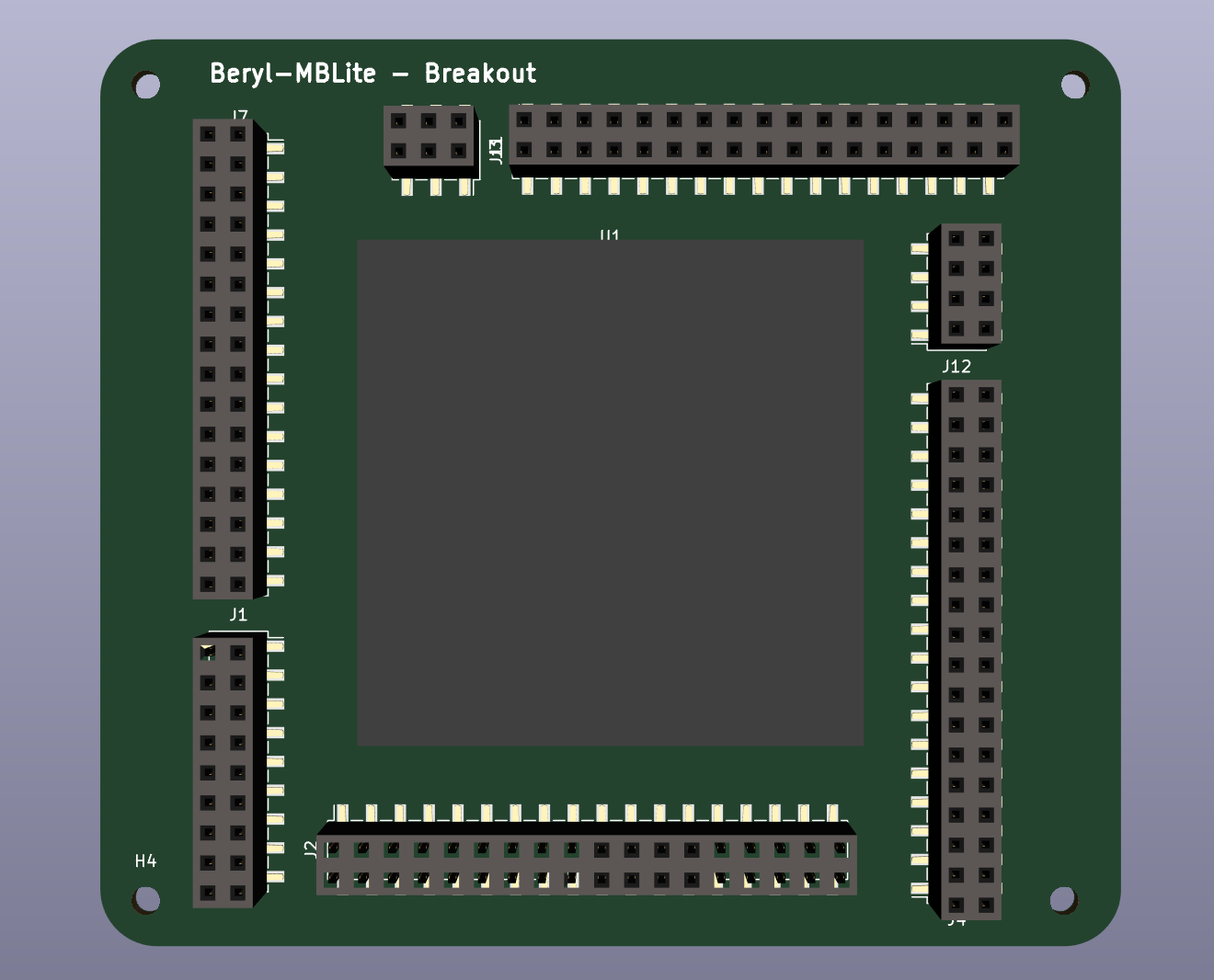
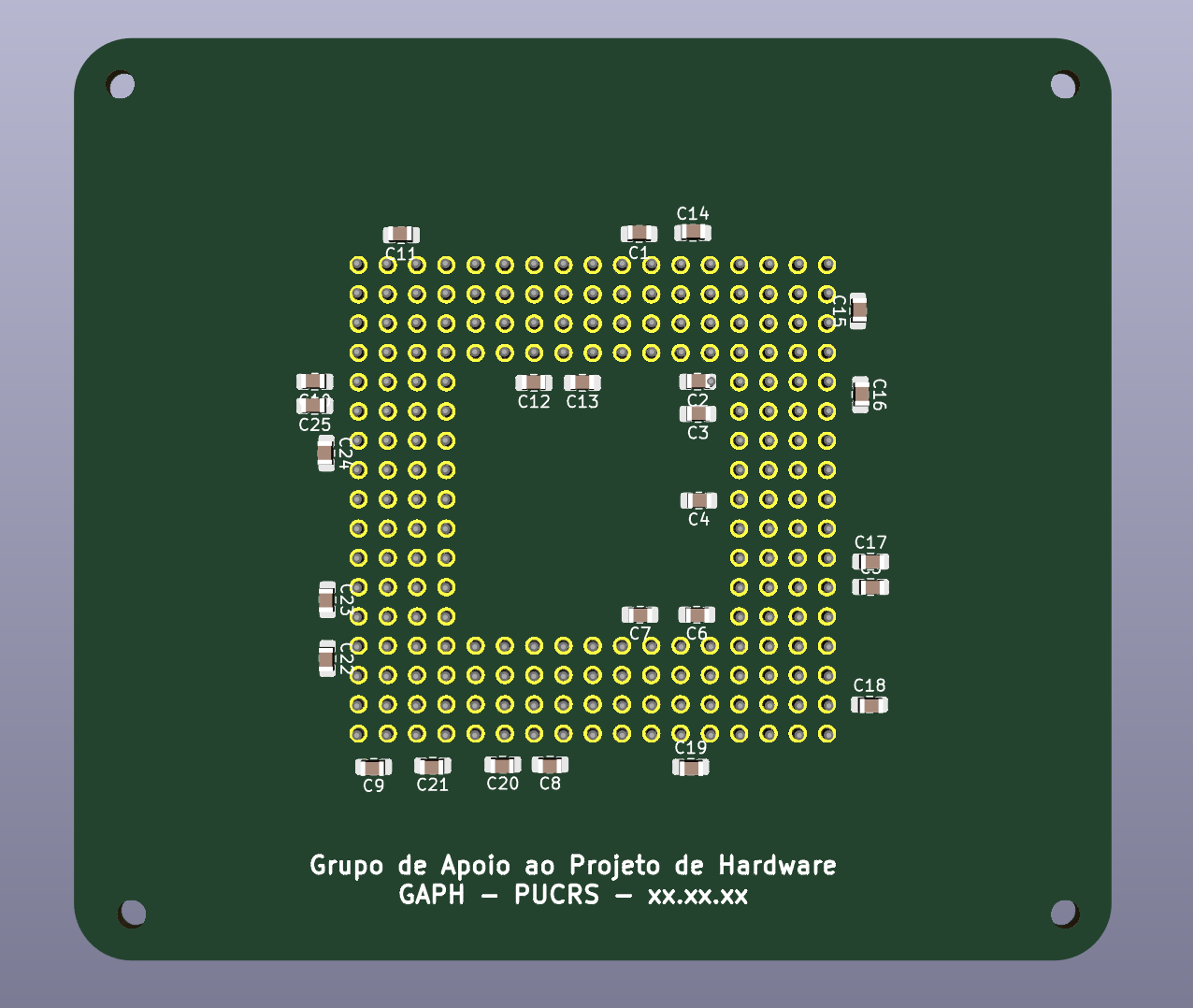
Beryl MBLite Soc was finished in March 2014 and can be accessed through GAPH's old SVN.
| Qty | Value | Footprint | References |
|---|---|---|---|
| 25 | 100n | Capacitor_SMD:C_0805_2012Metric_Pad1.15x1.40mm_HandSolder | C1, C2, C10, C11, C12, C13, C14, C15, C16, C17, C18, C19, C20, C21, C22, C23 +9 |
| 4 | MountingHole | MountingHole:MountingHole_2.5mm | H1, H2, H3, H4 |
| 2 | chip_data_mem_o_1 | Connector_PinSocket_2.54mm:PinSocket_2x18_P2.54mm_Vertical_SMD | J2, J4 |
| 1 | BERYL-MBLite | GAPH-Chips:PGA-290_17x17_43.18x43.18mm | U1 |
| 1 | Main | Connector_PinSocket_2.54mm:PinSocket_2x03_P2.54mm_Vertical_SMD | J11 |
| 1 | chip_inst_mem_o | Connector_PinSocket_2.54mm:PinSocket_2x09_P2.54mm_Vertical_SMD | J1 |
| 1 | data_mem_i | Connector_PinSocket_2.54mm:PinSocket_2x17_P2.54mm_Vertical_SMD | J3 |
| 1 | inst_mem_i | Connector_PinSocket_2.54mm:PinSocket_2x16_P2.54mm_Vertical_SMD | J7 |
| 1 | power | Connector_PinSocket_2.54mm:PinSocket_2x04_P2.54mm_Vertical_SMD | J12 |

AzonInc/Doorman
ESP32-S3 based Intercom Gateway (TCS / Koch / Niko / Scantron / Analogue Systems)


Xii-Labs/Xii-Boy-Ultra
The world's first wire-free Wii portable, now in the palm of your hands. Better than ever, optimized to delight, built for fun. The next generation of Wii portables starts now.


It measures 90 × 80 mm and has 4 copper layers, 1.6 mm thick.
37 parts. The full list of its parts is on this page, with links to each part's symbol and footprint where PCBKit's library has them.
From the leoheck/beryl-breakout repository on GitHub, at the commit this page was made from: the board is board.kicad_pcb. PCBKit opens the board in the browser, with nothing to install.
Its repository states no licence, so its author keeps all rights: ask leoheck before reusing the design.