2 layers140.5 × 30 mm
Type e
google/mozc-devices
Circuit diagrams and firmware source code for Gboard DIY keyboards
16 parts3kApache-2.0

 leoheck/KiCad-Design-Examples3
A simple line filter circuit implements individual clearances for phase-to-neutral, mains-to-earth, and earth to PCB edge clearances, as well as small self-clearances for nets that share the same DC potential, but may…
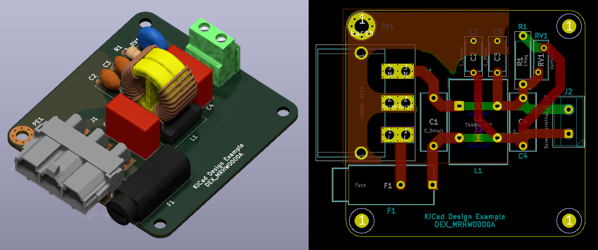
Dex0000 mains filter is an open-source printed circuit board by leoheck, from the leoheck/KiCad-Design-Examples repository on GitHub. It is a 2-layer board of 75 × 71 mm with 16 parts on 6 nets, routed with 68 tracks and 0 vias.
Its parts include 4 capacitors, 2 connectors, 1 resistor, 1 inductor and 1 fuse.
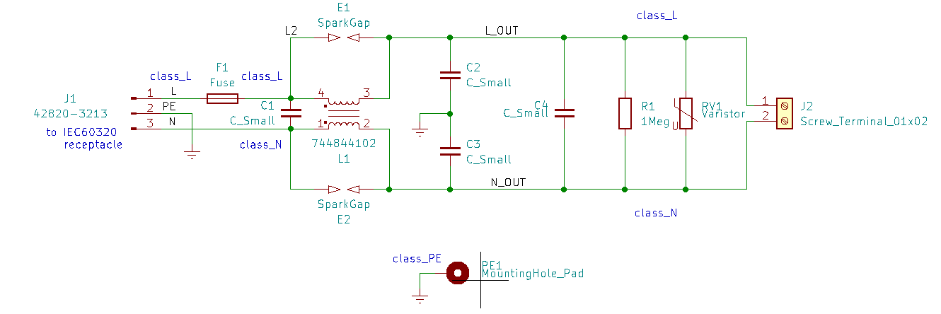
A simple line filter circuit implements individual clearances for phase-to-neutral, mains-to-earth, and earth to PCB edge clearances, as well as small self-clearances for nets that share the same DC potential, but may be split to account for AC behavior. The latter is applied hier to the case of a common-mode choke.
The Net Classes panel is used to
Clearance values given here can be superseded by rules written in Design Rules > Rules.
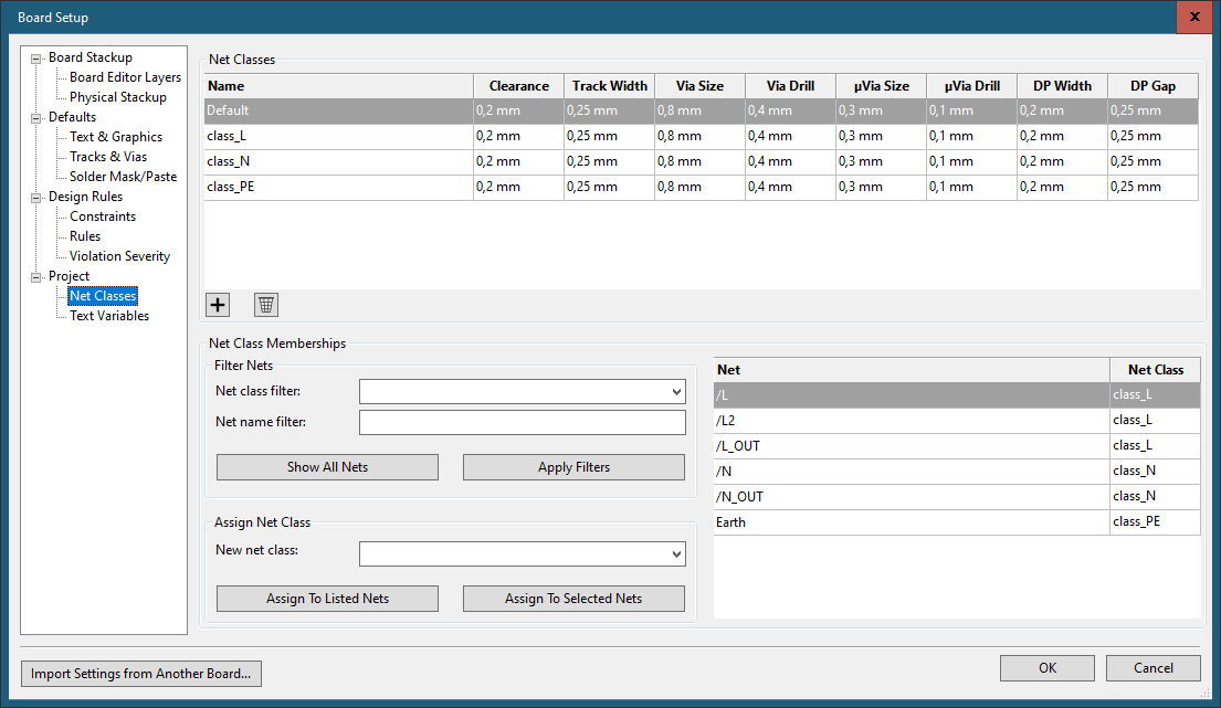
When specifying only a basic clearance value in the Net Classes table, this value becomes the distance any net item (track segment, pad, ...) must keep form items in other nets, no matter the net class. Between two items of net classes with differing clearance requirements, the larger clearance is applied.
An equivalent rule for class_x with 0.2mm clearance has the form
(rule "class_X"
    (condition "A.NetClass == 'class_X'")
    (constraint clearance (min 0.2mm)))
Such a rule written in Design Rules > Rules supersedes the implicit definition through the Net Classes table, but is functionally equivalent until the boolean expression it contains is extended. Meanwhile, the Net Classes table values cover all cases not otherwise described in the design rules script.
The distinction between same-class net and other-class net clearances is made by forming two complementary rules. A and B are the corresponding board items between which the clearance resolution is determined.
(rule "N_mutual_clearance"
    (condition "A.NetClass == 'class_N' && B.NetClass != A.NetClass")
    (constraint clearance (min 3.0mm)))

(rule "N_self_clearance"
    (condition "A.NetClass == 'class_N' && B.NetClass == A.NetClass")
    (constraint clearance (min 0.75mm)))
Finally, order-of-evaluation needs to be kept in mind. In the example below, clearance rules named r1-r6 for short are thought to be written in consecutive order, which leads to a chevron stack pattern in the associated clearance matrix. r1, r3, r5 are mutual clearance rules, r2, r4, r6 are same-class clearance rules:
step 1:					step 2:					step 3:
	X	Y	Z			X	Y	Z			X	Y	Z
X		r1	r1		X	r2	r1	r1		X	r2	r3	r1
Y	r1				Y	r1				Y	r3		r3
Z	r1				Z	r1				Z	r1	r3

step 4:					step 5:					step 6:
	X	Y	Z			X	Y	Z			X	Y	Z
X	r2	r3	r1		X	r2	r3	r5		X	r2	r3	r5
Y	r3	r4	r3		Y	r3	r4	r5		Y	r3	r4	r5
Z	r1	r3			Z	r5	r5			Z	r5	r5	r6
The roles of A and B in the rule description can be swapped, which makes the clearance matrix symmetric, so it's usually only given in triangle form.
In its most general form, clearance matrix elements can also be specified individually by writing out all (N²+N)/2 combinations of N net classes occuring in the design, including the diagonal ones:
(rule "clearance_<class_i>_<class_j>"
    (condition "A.NetClass == '<class_i>' && A.NetClass == '<class_j>'")
    (constraint clearance (min 0.2mm)))
where <class_i>, <class_j> are placeholders.
Design Rules can also describe constraints with respect to net classes not (yet) contained in the design. This may at a later stage be pointed out in the form of syntax check info messages. Always validate the correctness of the resulting clearances, for example by selecting two layout items and using Inspect > Clearance Resolution to see which rule and what clearance value was found to apply.
Please see the project files for the full list of rules. An excerpt is given below.
# Project Rules
#
# Phase is segmented to insert a fuse holder and one winding of a common-mode filter choke.
# A spark gap is inserted across the filter winding to prevent insulation breakdown in
# the event of a transient overvoltage condition. The same concept is applied to neutral.
#
# Clearance Matrix equivalent:
#
#			class_L		class_N		class_PE
#	class_L		0.75mm		3.0mm		4.5mm
#	class_N				0.75mm		4.5mm
#	class_PE					0.2mm*
#
# * Note there is only PE_mutual_clearance for clearance to other nets, so class_PE self-clearance
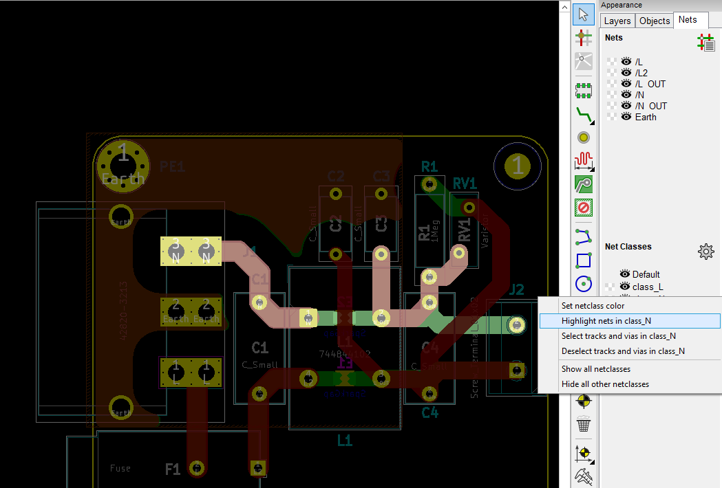
# defaults to 0.2mm from Project > Net Classes.All members of a net class can be highlighted by using the right-click option "Hightlight nets in " of a class listed in Appearance > Nets > Net Classes:
This project is part of a set of design examples. See https://github.com/MisterHW/KiCad-Design-Examples/ for more.
| Qty | Value | Footprint | References |
|---|---|---|---|
| 3 | MountingHole | MountingHole:MountingHole_4.3mm_M4_DIN965 | H1, H2, H3 |
| 2 | C_Small | Capacitor_THT:C_Disc_D9.0mm_W5.0mm_P10.00mm | C2, C3 |
| 2 | C_Small | Capacitor_THT:C_Rect_L18.0mm_W8.0mm_P15.00mm_FKS3_FKP3 | C1, C4 |
| 2 | SparkGap | sparkgaps:SG1210 | E1, E2 |
| 1 | 1Meg | Resistor_THT:R_Axial_DIN0414_L11.9mm_D4.5mm_P15.24mm_Horizontal | R1 |
| 1 | 42820-3213 | Connector_Molex:Molex_Mini-Fit_Sr_42820-32XX_1x03_P10.00mm_Horizontal_ThermalVias | J1 |
| 1 | 744844102 | Inductor_THT:WE-ExB | L1 |
| 1 | Fuse | Fuse:Fuseholder_Cylinder-5x20mm_Schurter_FAB_0031-355x_Horizontal_Closed | F1 |
| 1 | MountingHole_Pad | MountingHole:MountingHole_4.3mm_M4_Pad_Via | PE1 |
| 1 | Screw_Terminal_01x02 | TerminalBlock_MetzConnect:TerminalBlock_MetzConnect_Type171_RT13702HBWC_1x02_P7.50mm_Horizontal | J2 |
| 1 | Varistor | Varistor:RV_Disc_D12mm_W4.2mm_P7.5mm | RV1 |
google/mozc-devices
Circuit diagrams and firmware source code for Gboard DIY keyboards

conorpp/u2f-zero
U2F USB token optimized for physical security, affordability, and style

rusefi/rusefi
rusefi - GPL internal combustion engine control unit

VoronDesign/Voron-Hardware
Cool Hardware designed by the Voron Design group

hoglet67/RGBtoHDMI
Bare-metal Raspberry Pi project that provides pixel-perfect sampling of Retro Computer RGB/YUV video and conversion to HDMI

hackclub/OnBoard
💡 Join 1,000 teenagers and make your first PCB with a $100 grant!


It measures 75 × 71 mm and has 2 copper layers, 1.6 mm thick.
16 parts. The full list of its parts is on this page, with links to each part's symbol and footprint where PCBKit's library has them.
From the leoheck/KiCad-Design-Examples repository on GitHub, at the commit this page was made from: the board is dex0000_mains_filter/dex0000_mains_filter.kicad_pcb and its schematic dex0000_mains_filter/dex0000_mains_filter.kicad_sch. PCBKit opens the board in the browser, with nothing to install.
Its repository states no licence, so its author keeps all rights: ask leoheck before reusing the design.