

4 layers100 × 100 mm
Labathome pcb
klaus-liebler/labathome
Der kleine Bruder von lab@home. Ermöglicht das Experimentieren mit PT1...PTn-Gliedern, die intern als RC-Kombination (entkoppelt über Operationsverstärker) ausgeführt sind.
292 parts5MIT

Open-source RIAA phono preamp for the Bang & Olufsen BeoGram 4002/4004 turntable (KiCad)
RIAA is an open-source printed circuit board by leicht-io, from the leicht-io/BeoGram-4002-RIAA repository on GitHub, published under the CERN-OHL-S-2.0 licence. It is a 2-layer board of 112 × 202 mm with 63 parts on 55 nets, routed with 438 tracks and 23 vias.
It is built around the OPA2134UA/2K5, LM317D2TR4G-JSM and CL31A106KBHNNNE, with the FZ1V100M0506, MKS2C023301A00JSSD and CL31B104KBCNNNC among its other parts. Its parts include 26 resistors, 22 capacitors, 4 diodes, 3 ICs and 3 connectors. It belongs with the audio and music boards of this library.



An open-source RIAA phono preamplifier board for the Bang & Olufsen BeoGram 4002 / 4004 turntable, designed in KiCad.
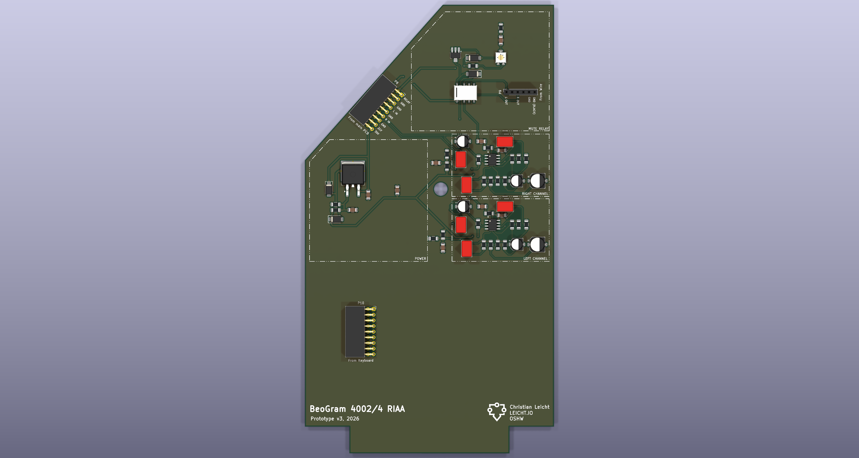
| Status | Prototype v3 (SMD) – designed, not built yet. v2 was manufactured and tested working. |
| Tool | KiCad 10 |
| Board | 2-layer, 1.6 mm, ~112 × 202 mm |
| Hardware licence | CERN-OHL-S v2 |
| Docs licence | CC BY-SA 4.0 |
This project is community driven. Build reports, measurements and design improvements are very welcome – see CONTRIBUTING.md. Questions and build help: Discussions.
A dual-stage active/passive RIAA equalizer per channel, based on the classic LM833 application topology but using the OPA2134 for lower distortion. Full details are in docs/design-notes.md.
VREF_L / VREF_R). Stage 1 is biased from it, so supply ripple is not amplified, and stage 2 is DC-coupled to stage 1. R103/R203 (47 k) also set the 47 kΩ cartridge load.RELAY ON signal has been present for a while. The delay is set with RV1, and the board mutes instantly when the signal drops. Q1 is a Darlington (BCV49), as on the original B&O board.
Simulated with nominal part values, an ideal source and a 47 kΩ amplifier input. It has not been measured yet.
| Frequency | v3 deviation from RIAA | v2 deviation from RIAA |
|---|---|---|
| 20 Hz | −0.63 dB | −0.85 dB |
| 50 Hz | −0.08 dB | −0.23 dB |
| 100 Hz | +0.03 dB | −0.12 dB |
| 1 kHz | 0 (reference) | 0 (reference) |
| 10 kHz | −0.02 dB | +0.70 dB |
| 20 kHz | −0.03 dB | +0.73 dB |
The roll-off below 50 Hz comes from the coupling capacitors. Real boards also vary with the 5 % tolerance of the RIAA film capacitors. To regenerate the chart after changing values, edit them in scripts/riaa_response.py and run python3 scripts/riaa_response.py images/riaa-response.svg.
The board takes the place of B&O's PCB 8, the muting module (8005014 in the 4002, 8005022 with remote control in the 4004). Pin n of the original 9-pin P8 and P10 is pins 2n−1 and 2n here.
P8 – From main PCB (2×9, 2.54 mm)
| Pin | Signal |
|---|---|
| 1, 2 | RELAY ON |
| 3, 4 | GND (main board) |
| 5, 6 | Pickup cable shields (GND) |
| 7, 8 | L IN (pickup) |
| 9, 10 | L pickup return (joins GND only at NT1) |
| 11, 12 | R IN (pickup) |
| 13, 14 | R pickup return (joins GND only at NT2) |
| 15, 16 | 21 V (relay supply) |
| 17, 18 | 30 V (preamp supply) |
P10 – From Keyboard (2×9, 2.54 mm). Power only; the other pins are not connected. Like the original module, the board passes 30 V, 21 V and GND from P8 through to the keyboard.
| Pin | Signal |
|---|---|
| 3, 4 | 30 V |
| 11, 12 | 21 V |
| 13, 14 | GND |
P9 – Output (1×6, 2.54 mm). Same pin layout as the original P9, so the turntable's own output harness fits.
| Pin | Signal |
|---|---|
| 1 | L OUT (DIN pin 3) |
| 3 | R OUT (DIN pin 5) |
| 5 | GND, signal ground (DIN pin 2) |
| 6 | GND, chassis |
| 2, 4 | Not connected (Beomaster 2400 remote lines on a 4004, see below) |
BeoGram 4004: the 4004's PCB 8 (8005022) also holds the remote-control circuit for a Beomaster 2400 (start, pause and stop from the PHONO and STAND BY keys). This board doesn't have it:
Gerbers and other fabrication files are not committed to the repository. CI generates them from the KiCad sources on every push, so they always match the design:
v*) has a GitHub release with the gerber zip, a schematic PDF, the BOMs, the pick-and-place files and renders.main / any PR: open the latest KiCad workflow run and download the fabrication artifact (you must be logged in to GitHub).kicad-cli commands from .github/workflows/kicad.yml.The gerbers of the first (v1) prototype are no longer in the tree but remain in the git history.
The CI produces these BOMs and pick-and-place (CPL) files:
| File | Contents |
|---|---|
RIAA-bom-full.csv | Every part, with manufacturer, manufacturer part number (MPN) and LCSC number. The Assembly column says whether a part is assembled by JLCPCB or soldered by hand. |
RIAA-bom-jlcpcb.csv + RIAA-cpl-jlcpcb.csv | Upload-ready files for JLCPCB SMT assembly (parts from LCSC; film capacitors excluded). |
RIAA-bom-pcbway.csv + RIAA-cpl-pcbway.csv | Upload-ready files for PCBWay turnkey assembly. The BOM lists every part, including the film capacitors and connectors, by manufacturer and MPN, with the LCSC number as distributor part number. The CPL lists the surface-mount parts. |
Every part in the schematic has Manufacturer and MPN fields; parts JLCPCB can place also have an LCSC PN field.
Order the board with assembly from one of the two fabs:
RIAA-bom-jlcpcb.csv and RIAA-cpl-jlcpcb.csv. The film capacitors are not included (step 2).RIAA-bom-pcbway.csv and RIAA-cpl-pcbway.csv. PCBWay sources every part, including the through-hole film capacitors and connectors, so step 2 is not needed.Check the part rotations and the polarity of the diodes and electrolytic capacitors in the fab's preview before confirming. Stock of the 0.1 % resistors in the RIAA network is low at times. A 1 % part of the same value is fine if one runs out.
For a JLCPCB board, hand-solder the parts marked Hand in RIAA-bom-full.csv: the film capacitors C101, C102, C105 and C201, C202, C205. C102/C202 and C105/C205 set the RIAA time constants, so tight-tolerance or matched parts give the most accurate curve.
Set RV1 for the unmute delay you want (about 1 s to 10 s).
Install it in the turntable. An illustrated installation guide is still missing – contributions are very welcome.
Please post a Build report issue when you have built one, whether it worked or not.
RIAA.kicad_pro / .kicad_sch / .kicad_pcb   KiCad project
parts/                                     Project-local footprints (OPA2134 D8)
3d-parts/                                  STL files for the 3D-printed board guides
docs/                                      Design notes
images/                                    Renders and photos
scripts/make_bom.py                        Builds the full, JLCPCB and PCBWay BOMs and CPL files (used by CI)
scripts/riaa_response.py                   Simulates the RIAA response and draws images/riaa-response.svg
.github/ CI workflow, issue and PR templatesSee CONTRIBUTING.md. In short: open an issue or discussion first for design changes, keep each PR focused, and include screenshots of what you changed in the schematic or PCB.
This board connects to the turntable's internal 30 V supply. Vintage equipment can be damaged by wiring mistakes. Everything here is provided as is, without any warranty (see the licence), and you build and install it at your own risk.
Bang & Olufsen, BeoGram and related names are trademarks of their owners. This project is not affiliated with or endorsed by Bang & Olufsen.
scripts/): GPL-3.0-or-laterChristian Leicht – leicht.io
| Qty | Value | Footprint | References |
|---|---|---|---|
| 5 | 100k | Resistor_SMD:R_1206_3216Metric_Pad1.30x1.75mm_HandSolder | R22, R23, R24, R25, R26 |
| 4 | 10uF | Capacitor_SMD:C_1206_3216Metric_Pad1.33x1.80mm_HandSolder | C1, C30, C107, C207 |
| 4 | 10uF | Capacitor_SMD:CP_Elec_5x5.4 | C106, C108, C206, C208 |
| 4 | 33nF | Capacitor_THT:C_Rect_L7.2mm_W4.5mm_P5.00mm_FKS2_FKP2_MKS2_MKP2 | C102, C105, C202, C205 |
| 3 | 100nF | Capacitor_SMD:C_1206_3216Metric_Pad1.33x1.80mm_HandSolder | C27, C28, C29 |
| 3 | 1N4004 | Diode_SMD:D_SMA | D5, D7, D8 |
| 2 | 100 | Resistor_SMD:R_1206_3216Metric_Pad1.30x1.75mm_HandSolder | R113, R213 |
| 2 | 100pF | Capacitor_THT:C_Rect_L7.2mm_W4.5mm_P5.00mm_FKS2_FKP2_MKS2_MKP2 | C101, C201 |
| 2 | 10k | Resistor_SMD:R_1206_3216Metric_Pad1.30x1.75mm_HandSolder | R106, R206 |
| 2 | 2.37k | Resistor_SMD:R_1206_3216Metric_Pad1.30x1.75mm_HandSolder | R107, R207 |
| 2 | 220uF | Capacitor_SMD:CP_Elec_6.3x7.7 | C103, C203 |
| 2 | 22uF | Capacitor_SMD:C_1206_3216Metric_Pad1.33x1.80mm_HandSolder | C34, C35 |
| 2 | 2k | Resistor_SMD:R_1206_3216Metric_Pad1.30x1.75mm_HandSolder | R110, R210 |
| 2 | 47k | Resistor_SMD:R_1206_3216Metric_Pad1.30x1.75mm_HandSolder | R103, R203 |
| 2 | 54.9k | Resistor_SMD:R_1206_3216Metric_Pad1.30x1.75mm_HandSolder | R108, R208 |
| 2 | 590 | Resistor_SMD:R_1206_3216Metric_Pad1.30x1.75mm_HandSolder | R104, R204 |
| 2 | 7.5k | Resistor_SMD:R_1206_3216Metric_Pad1.30x1.75mm_HandSolder | R109, R209 |
| 2 | 95.3k | Resistor_SMD:R_1206_3216Metric_Pad1.30x1.75mm_HandSolder | R105, R205 |
| 2 | NetTie_2 | NetTie:NetTie-2_SMD_Pad0.5mm | NT1, NT2 |
| 2 | OPA2134 | OPA2134:D8 | U5, U6 |
| 1 | 100uF/6.3V | Capacitor_SMD:C_1206_3216Metric_Pad1.33x1.80mm_HandSolder | C33 |
| 1 | 1M | Potentiometer_SMD:Potentiometer_Bourns_3314G_Vertical | RV1 |
| 1 | 1N4002 | Diode_SMD:D_SMA | D6 |
| 1 | 1k | Resistor_SMD:R_1206_3216Metric_Pad1.30x1.75mm_HandSolder | R21 |
| 1 | 300 | Resistor_SMD:R_1206_3216Metric_Pad1.30x1.75mm_HandSolder | R20 |
| 1 | 4k7 | Resistor_SMD:R_1206_3216Metric_Pad1.30x1.75mm_HandSolder | R19 |
| 1 | BCV49 | Package_TO_SOT_SMD:SOT-89-3_Handsoldering | Q1 |
| 1 | From Keyboard | Connector_PinSocket_2.54mm:PinSocket_2x09_P2.54mm_Horizontal | P10 |
| 1 | From Wire | Connector_PinSocket_2.54mm:PinSocket_1x06_P2.54mm_Vertical | P9 |
| 1 | From main PCB | Connector_PinSocket_2.54mm:PinSocket_2x09_P2.54mm_Horizontal | P8 |
| 1 | G6K-2F-Y DC24 | Relay_SMD:Relay_DPDT_Omron_G6K-2F-Y | K1 |
| 1 | LM317 | Package_TO_SOT_SMD:TO-263-2 | U7 |
klaus-liebler/labathome
Der kleine Bruder von lab@home. Ermöglicht das Experimentieren mit PT1...PTn-Gliedern, die intern als RC-Kombination (entkoppelt über Operationsverstärker) ausgeführt sind.

kenyattaejones32-boop/Gasmat_Gateway
KiCad 8 hardware design for the Gasmat Gateway board (Geviton).

researchanddesire/assembly-docs
RAD unified assembly docs — ohai.researchanddesire.com

Celcius1/Old-Projects-become-New
Electronics Projects from the 60's to 90's redone for the modern era


ArgonautGit/wallet_dmm
A multimeter the size of a credit card: DC volts, resistance, continuity and diode test, shown on a 0.91" OLED, with three buttons, an RGB LED and a piezo beeper.

It measures 112 × 202 mm and has 2 copper layers, 1.6 mm thick.
63 parts, built around the OPA2134UA/2K5, LM317D2TR4G-JSM, CL31A106KBHNNNE and FZ1V100M0506. The full list of its parts is on this page, with links to each part's symbol and footprint where PCBKit's library has them.
From the leicht-io/BeoGram-4002-RIAA repository on GitHub, at the commit this page was made from: the board is RIAA.kicad_pcb and its schematic RIAA.kicad_sch. PCBKit opens the board in the browser, with nothing to install.
Its repository publishes it under the CERN-OHL-S-2.0 licence: you may reuse it on that licence's terms (keep the author's notice, and for a copyleft licence share your changes alike).