2 layers25.5 × 24.6 mm
Board b
leakydata/bme690-toolkit
Toolkit for the BME-690 sensor array on a Bosch Application Board 3.1 shuttle board.
16 partsMIT

 leakydata/bme690-toolkit
Toolkit for the BME-690 sensor array on a Bosch Application Board 3.1 shuttle board.
Board a is an open-source printed circuit board by leakydata, from the leakydata/bme690-toolkit repository on GitHub, published under the MIT licence. It is a 2-layer board of 29.3 × 26.2 mm with 15 parts on 19 nets, routed with 168 tracks and 5 vias.
Its parts include 4 capacitors, 4 resistors and 3 connectors.
A 29.3 x 26.2 mm board that takes any Bosch Sensortec Shuttle Board 3.0, including the BME690 8x shuttle, and brings all 16 of its pins out to a labelled 2.54 mm header for Dupont wires, a breadboard ribbon or a microcontroller.
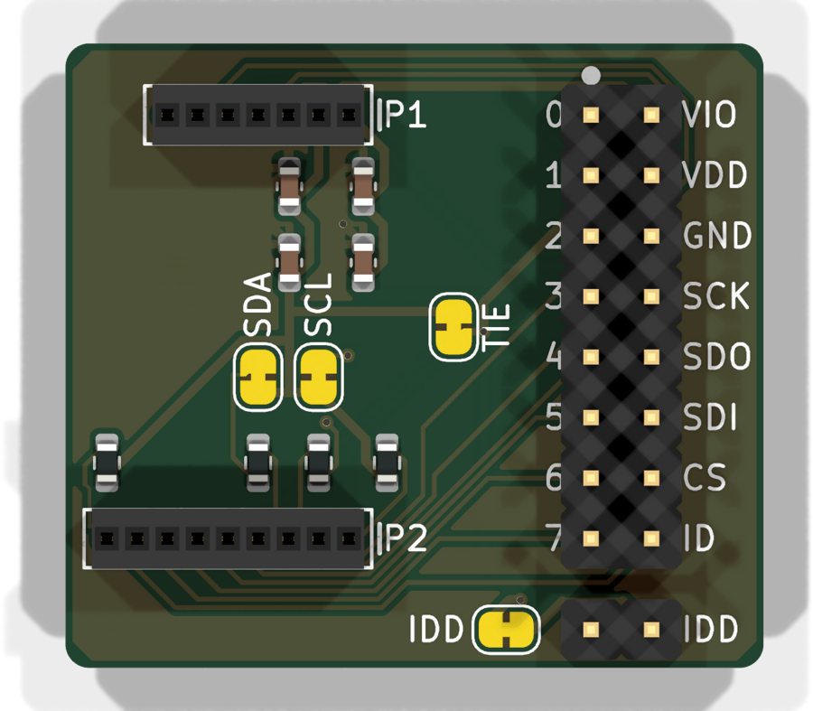
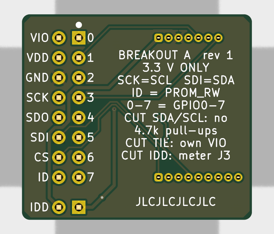
| part | job |
|---|---|
| J1 | shuttle sockets: P1 (7 pins) and P2 (9 pins), 1.27 mm. A 7-pin and a 9-pin socket, so the shuttle only fits one way |
| J2 | 2x8 2.54 mm header with every shuttle pin |
| J3 | 2 pins for measuring the sensor's VDD current (IDD) |
| R1, R2 | 4.7k I2C pull-ups on SDA and SCL, each behind a cut jumper |
| R3 | 1k pull-up on PROM_RW, the shuttle's ID chip |
| R4 | 10k pull-up on CS, so single-sensor shuttles start in I2C mode |
| C1-C4 | 100 nF + 10 uF on VDD, and the same on VDDIO |
3.3 V only. Never connect 5 V.
The column next to the shuttle carries its GPIO0-7, and the outer column carries power and the bus. Both sides of the board are labelled, and a dot marks pin 1.
| row | inner pin | inner label | signal | outer pin | outer label | signal |
|---|---|---|---|---|---|---|
| 1 | 1 | 0 | GPIO0 (P1-4) | 2 | VIO | VDDIO (P1-2) |
| 2 | 3 | 1 | GPIO1 (P1-5) | 4 | VDD | VDD supply in |
| 3 | 5 | 2 | GPIO2/INT1 (P1-6) | 6 | GND | GND (P1-3) |
| 4 | 7 | 3 | GPIO3/INT2 (P1-7) | 8 | SCK | SCK/SCL (P2-2) |
| 5 | 9 | 4 | GPIO4 (P2-5) | 10 | SDO | SDO (P2-3) |
| 6 | 11 | 5 | GPIO5 (P2-6) | 12 | SDI | SDI/SDA (P2-4) |
| 7 | 13 | 6 | GPIO6 (P2-7) | 14 | CS | CS (P2-1) |
| 8 | 15 | 7 | GPIO7 (P2-8) | 16 | ID | PROM_RW (P2-9) |
On the BME690 8x shuttle, GPIO0-7 are the chip selects of sensors U1-U8, and CS (P2-1) isn't connected to anything. The 8x shuttle only works over SPI: in I2C mode all eight sensors would answer at the same address.
All four are closed as made. To open one, cut the thin trace between its pads with a sharp knife. To close it again, bridge the pads with solder.
| jumper | label | open it to |
|---|---|---|
| JP1 | IDD (bottom left of J3) | measure sensor current: put a meter across J3 |
| JP2 | TIE | power VDDIO separately from VDD (feed VIO yourself) |
| JP3 | SDA | remove the 4.7k SDA pull-up |
| JP4 | SCL | remove the 4.7k SCL pull-up |
With TIE closed, one 3.3 V wire to VIO or VDD powers everything.
The header is hand-soldered, so you choose:
To a breadboard: use a 16-way ribbon cable with a 2x8 IDC socket on one end and a 16-pin DIP IDC plug on the other. Put the red stripe at the pin-1 dot. The plug sits across the breadboard's centre gap. Its pins alternate between the two DIP rows, so check the plug's datasheet for which conductor lands where. A flat ribbon also passes a jar lid's seal far better than loose jumpers.
JLCPCB fits the eight 0603 parts. You solder the through-hole parts.
smoke_test/smoke_test.ino (Arduino IDE or arduino-cli, ESP32 core 3.x,
board "ESP32S3 Dev Module"). The wiring matches the logger firmware's pin
map, so a board wired for the logger runs the test unchanged.
| Board A | ESP32-S3 |
|---|---|
| VIO | 3V3 |
| GND | GND |
| SCK | GPIO12 |
| SDI | GPIO11 |
| SDO | GPIO13 |
| 0-7 | GPIO1, 2, 4, 5, 6, 7, 15, 16 |
MODE_SPI 1 (the default), for the 8x shuttle: reads the chip ID
register of all eight sensors and expects 0x61 from each. A sensor
that answers wrong names its chip-select wire.MODE_SPI 0, for a single-sensor shuttle: scans I2C and reads register
0xD0 at 0x76. It drives SDO low to set that address, because SDO
must not float. Expect 0x61. Leave CS open; the 10k pull-up selects I2C.For the full logger, see firmware/bme690-logger-idf.
PROM_RW (shuttle ID): the DS28E05 talks at 1-Wire overdrive speed only (up to 76.9 kbps). The datasheet's overdrive timings are:
| timing | value |
|---|---|
| reset low | 48-80 us |
| presence sample | 8-10 us |
| write-0 low | 8-16 us |
| write-1 / read low | 1-2 us |
| sample by | 2 us |
| slot | 13 us minimum |
| EEPROM write | 16 ms per write |
Common ESP32 1-Wire libraries run at standard speed and won't see it. A reader needs these timings, using the RMT peripheral or interrupt-free bit timing. It isn't in the smoke test yet.
All files are in fab/:
| file | upload as |
|---|---|
board_a-gerbers.zip | the PCB (Gerbers + Excellon drill) |
board_a-bom-jlcpcb.csv | PCB Assembly: BOM |
board_a-cpl-jlcpcb.csv | PCB Assembly: CPL / pick-and-place |
board_a-bom-full.csv | your shopping list, including the hand-soldered parts |
board_a-schematic.pdf, board_a-layout.pdf | for checking |
Board options:
| option | setting |
|---|---|
| layers | 2 |
| thickness | 1.6 mm |
| material | FR-4 |
| solder mask | green |
| surface finish | LeadFree HASL |
| Mark on PCB | Remove Mark (free, and the default) |
| quantity | 5 |
Assembly options:
| option | setting |
|---|---|
| type | Economic |
| side | Top |
| boards to assemble | 5 (or 2, the minimum) |
All are LCSC Basic parts, so there is no extended-part fee. Stock was checked 2026-10-05.
| parts | value | LCSC | stock |
|---|---|---|---|
| R1, R2 | 4.7k 1% 0603 | C23162 | 22.2 M |
| R3 | 1k 1% 0603 | C21190 | 21.3 M |
| R4 | 10k 1% 0603 | C25804 | 29.6 M |
| C1, C3 | 100 nF X7R 50 V 0603 | C14663 | 57.2 M |
| C2, C4 | 10 uF X5R 10 V 0603 | C19702 | 10.3 M |
Per board:
| part | qty | about |
|---|---|---|
| Sullins LPPB071NFFN-RC, 7-pin 1.27 mm socket | 1 | $1.00 |
| Sullins LPPB091NFFN-RC, 9-pin 1.27 mm socket | 1 | $1.20 |
| 2x8 male header, 2.54 mm (straight or right angle) | 1 | $0.30 |
| 1x2 male header, 2.54 mm (optional, for IDD) | 1 | $0.05 |
These are estimates from JLCPCB's published prices (October 2026). The quote page gives the real figure.
| bare PCB | PCB + assembly | |
|---|---|---|
| 5 PCBs, 2-layer, under 100 x 100 mm | $2 | $2 |
| lead-free HASL surcharge | about $1-1.50 | about $1-1.50 |
| assembly setup (Economic) | - | $8.18 |
| stencil | - | $1.53 |
| solder joints, 80 x $0.0016 | - | $0.13 |
| parts: 5 Basic lines, LCSC minimum quantities | - | about $0.50-1 |
| extended-part fees | - | $0 (none) |
| subtotal before shipping | about $3-4 | about $13-15 |
| US shipping, Global Standard Direct (slowest, cheapest) | about $1.50-4 | about $2-5 |
| US shipping, DHL / UPS / FedEx express | about $15-25 | about $15-25 |
| US import duty (DDP, pre-collected) | a few dollars | a few dollars |
Plus about $13 for the hand-soldered parts for 5 boards, with distributor shipping on top.
Duties. JLCPCB ships to US individuals DDP (Delivered Duty Paid): the import duty is calculated and charged at checkout, so nothing is due on delivery. It is mandatory for individual customers. Business accounts may choose CPT and pay duty themselves. JLCPCB revised its US rates on 2026-03-17, after the February 2026 tariff change. The exact amount appears on the checkout page.
Coupons.
board_a-gerbers.zip. The viewer should show 29.3 x 26.2 mm,
2 layers and 39 holes, with the labels readable on both sides.JLCPCB 2-layer capabilities (jlcpcb.com/capabilities, checked 2026-10-03), with these values used:
| rule | used | JLCPCB minimum |
|---|---|---|
| clearance | 0.15 mm | 0.10 mm |
| minimum track | 0.15 mm (0.2 signal, 0.4 power) | 0.10 mm |
| vias | 0.6 mm pad, 0.3 mm hole | 0.25 / 0.15 mm |
| PTH annular ring | at least 0.225 mm (sockets) | 0.18 mm (0.25 recommended) |
| copper to board edge | 0.3 mm | 0.2 mm |
| hole to hole | 0.5 mm | 0.45 mm |
| silkscreen text | 1.0 mm high, 0.15 mm line | 1.0 / 0.15 mm |
ERC: 0 errors, 0 warnings. DRC, including warnings and schematic parity: 0.
Open board_a.kicad_pro in KiCad 10. build.py and pcb.py generated
the first version: one parts list feeds both the schematic and the board,
with Freerouting for the tracks. Once you edit in KiCad, keep editing there.
Re-running the scripts overwrites your changes. The shared symbols and
footprints are in ../shuttle_lib.
| Qty | Value | Footprint | References |
|---|---|---|---|
| 2 | 100nF | Capacitor_SMD:C_0603_1608Metric | C1, C3 |
| 2 | 10uF | Capacitor_SMD:C_0603_1608Metric | C2, C4 |
| 2 | 4.7k | Resistor_SMD:R_0603_1608Metric | R1, R2 |
| 1 | 10k | Resistor_SMD:R_0603_1608Metric | R4 |
| 1 | 1k | Resistor_SMD:R_0603_1608Metric | R3 |
| 1 | 2x8 header | Connector_PinHeader_2.54mm:PinHeader_2x08_P2.54mm_Vertical | J2 |
| 1 | IDD | Jumper:SolderJumper-2_P1.3mm_Bridged_RoundedPad1.0x1.5mm | JP1 |
| 1 | IDD meter | Connector_PinHeader_2.54mm:PinHeader_1x02_P2.54mm_Vertical | J3 |
| 1 | SCL pull-up | Jumper:SolderJumper-2_P1.3mm_Bridged_RoundedPad1.0x1.5mm | JP4 |
| 1 | SDA pull-up | Jumper:SolderJumper-2_P1.3mm_Bridged_RoundedPad1.0x1.5mm | JP3 |
| 1 | Shuttle 3.0 sockets | Shuttle3:Bosch_Shuttle_3.0_Sockets | J1 |
| 1 | TIE | Jumper:SolderJumper-2_P1.3mm_Bridged_RoundedPad1.0x1.5mm | JP2 |
leakydata/bme690-toolkit
Toolkit for the BME-690 sensor array on a Bosch Application Board 3.1 shuttle board.

google/mozc-devices
Circuit diagrams and firmware source code for Gboard DIY keyboards

hoglet67/RGBtoHDMI
Bare-metal Raspberry Pi project that provides pixel-perfect sampling of Retro Computer RGB/YUV video and conversion to HDMI

mntmn/amiga2000-gfxcard
MNT VA2000, an Open Source Amiga 2/3/4000 Graphics Card (Zorro II/III), written in Verilog

hackclub/OnBoard
💡 Join 1,000 teenagers and make your first PCB with a $100 grant!

kenp-io/not-for-airpods-repairs
The content of this repository is licensed under the WTFPL License. Please have a close look at the terms before using this material.

Luos-io/luos_engine
Open-source and real-time orchestrator for cyber-physical-systems, to easily design, test and deploy embedded applications and digital twins.

Chrismettal/EleLab_v2
Cheap DIY lab system for hobbyists and the tinkering folk

It measures 29.3 × 26.2 mm and has 2 copper layers, 1.6 mm thick.
15 parts. The full list of its parts is on this page, with links to each part's symbol and footprint where PCBKit's library has them.
From the leakydata/bme690-toolkit repository on GitHub, at the commit this page was made from: the board is board_a/board_a.kicad_pcb and its schematic board_a/board_a.kicad_sch. PCBKit opens the board in the browser, with nothing to install.
Its repository publishes it under the MIT licence: you may reuse it on that licence's terms (keep the author's notice, and for a copyleft licence share your changes alike).