
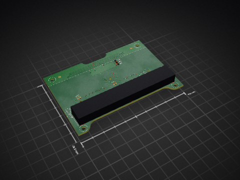
2 layers101.6 × 32.4 mm

 lambdakb/keyboard-lk56hs1
LK56HS 55% Staggered Keyboard
Lk56hs pcb is an open-source printed circuit board by lambdakb, from the lambdakb/keyboard-lk56hs repository on GitHub, published under the CERN-OHL-S-2.0 licence. It is a 2-layer board of 247.7 × 95.3 mm with 152 parts on 94 nets, routed with 594 tracks and 67 vias.
Its parts include 78 switches, 60 diodes, 2 capacitors, 2 connectors and 1 IC. It belongs with the keyboards and input boards and the RP2040 boards of this library.



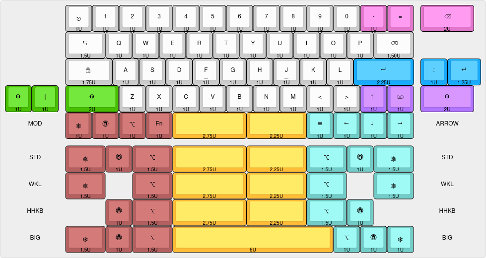
| PCB (Front) | PCB (Back) |
|---|---|
 |  |
The PCB has been designed in KiCad EDA 9.0 using the kicad-lkbd libraries and kbplacer.
You can preview the project files using KiCanvas directly in your browser and download the latest fabrication files for JLCPCB from the latest release.
The exported schematic is also available under output/schematics.
| Parameters | Value |
|---|---|
| Base Material | FR4 |
| Layers | 2 |
| Dimensions | 247.65 × 95.25 mm |
| PCB Thickness | 1.6 mm |
| PCB Color | Blue |
| Silkscreen | White |
| Surface Finish 1 | Lead Free HASL or ENIG |
| Copper Weight | 1 oz |
| Via Covering | Tented |
| Min Via Hole Size | 0.3 mm |
| Board Outline Tolerance | ± 0.2 mm |
| Plate (Top) | Plate (Bottom) |
|---|---|
 |  |
The plate has also been designed in KiCad EDA 9.0 using the kicad-lkbd libraries.
It is reversible, so you can choose to either have a wave pattern design shown or just a plain PCB plate. It can be used alongside another Keyboard PCB to create a full case by stacking:
Use the same parameters present in PCB Order to order the plate and bottom PCB, you can find the fabrication files in output/plate/fabrication/jlcpcb.
Be careful, JLCPCB may charge an extra fee for this PCB because it has "too many holes". You may want to prefer 3D printing a full case instead.
If you prefer to fabricate it by any other mean (such as laser cut acrylic), you can download their board outlines as DXF in output/plate/dxf.
The "HASL (with lead)" option is extremely discouraged due to the risk of lead poisoning. We strongly recommend paying the premium for the "Lead Free HASL" option. ↩
| Qty | Value | Footprint | References |
|---|---|---|---|
| 70 | SW_Push | LKBD_KeySwitch:SW_MX_HotSwap_nSilk | SW2, SW10, SW11, SW12, SW13, SW14, SW15, SW16, SW17, SW18, SW19, SW20, SW21, SW22, SW23, SW24 +54 |
| 60 | D | LKBD_Common:Diode_SMD_SOD-123_inSilk | D1, D2, D10, D11, D12, D14, D15, D16, D17, D18, D19, D20, D21, D22, D23, D24 +44 |
| 8 | MountingHole | LKBD_MountingHole:MountingHole_M2_NoPad | H1, H2, H3, H4, H5, H6, H7, H8 |
| 6 | MX_stab | LKBD_StabMX:Stabilizer_MX_2U | S13, S38, S41, S53, S62, S64 |
| 2 | 100nF | LKBD_Common:Capacitor_SMD_1206_inSilk | C1, C2 |
| 1 | JLCPCB_2DBarcode_8x8mm | LKBD_PCBFab:JLCPCB_2DBarcode_8x8mm | FAB1 |
| 1 | MX_stab | LKBD_StabMX:Stabilizer_MX_6U | S63 |
| 1 | PINHD_1x03_ARGB | LKBD_Connector:PinHeader_1x03_THT_P2.54mm_nSilk | J2 |
| 1 | PINHD_1x05_I2C | LKBD_Connector:PinHeader_1x05_THT_P2.54mm_nSilk | J3 |
| 1 | RaspberryPi_Pico | LKBD_MCU:MCU_RaspberryPi_Pico_THT | U1 |
| 1 | RotaryEncoder_Switch_MP | LKBD_KeySwitch:SW_MX_EC11_HotSwap_nSilk | SW1 |

TweetyDaBird/Lotus-58-Classic
A split ergo linear keyboard derived from the Lily58 family


ktec-hq/ErgoDone
ErgoDox using pro micro. Original work by Dox. Brainhole association present


It measures 247.7 × 95.3 mm and has 2 copper layers, 1.6 mm thick.
152 parts. The full list of its parts is on this page, with links to each part's symbol and footprint where PCBKit's library has them.
From the lambdakb/keyboard-lk56hs repository on GitHub, at the commit this page was made from: the board is pcb/lk56hs-pcb.kicad_pcb and its schematic pcb/lk56hs-pcb.kicad_sch. PCBKit opens the board in the browser, with nothing to install.
Its repository publishes it under the CERN-OHL-S-2.0 licence: you may reuse it on that licence's terms (keep the author's notice, and for a copyleft licence share your changes alike).