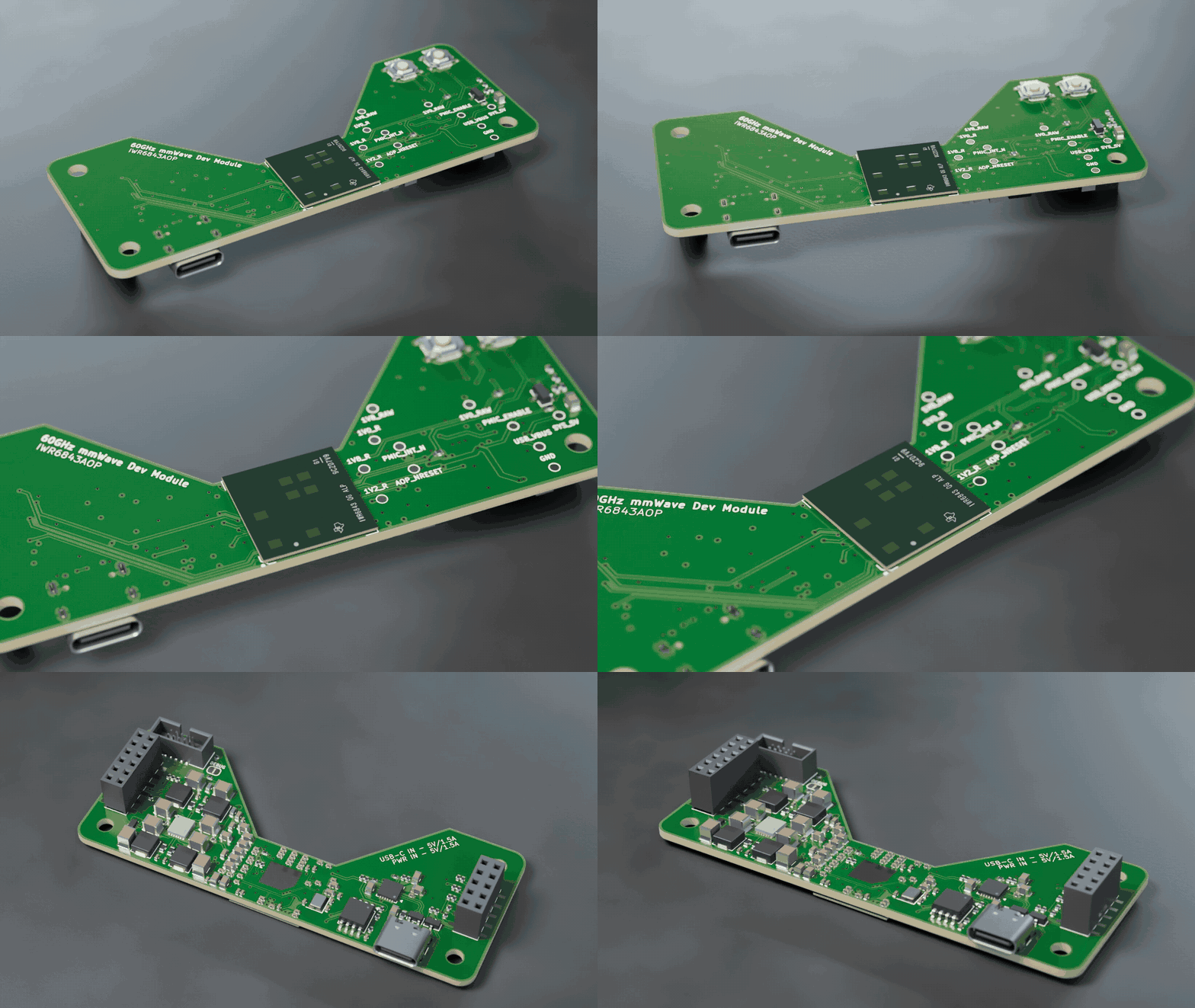
IWR AOP MODULE is an open-source printed circuit board by l3wi, from the l3wi/IWR-AOP-MODULE repository on GitHub, published under the MIT licence. It is a 6-layer board of 85.6 × 33.7 mm with 158 parts on 129 nets, routed with 944 tracks and 203 vias.
It is built around the IWR6843ARQGALPR, CP2105-F01-GMR and LP87524JRNFRQ1, with the MX25L3233FM2I-08G, MWSA0402S-R47MT and 0402CG180J500NT among its other parts. Its parts include 77 capacitors, 43 resistors, 5 ICs, 4 connectors and 4 inductors.
Revision 1.0 · KiCad 10 · six-layer, 85.6 × 33.7 mm · in production
A self-contained 60 GHz mmWave radar module built around TI's IWR6843AOP (antenna-on-package). It boots its own firmware from on-board flash and connects to a PC over USB-C or a carrier through two rear sockets.
Features
Radar. IWR6843AOP: 60–64 GHz FMCW, 4 GHz continuous sweep, 3 transmitters and 4 receivers with antennas in the package, C674x DSP, hardware FFT/CFAR accelerator and Arm Cortex-R4F. Detection and tracking run on the radar; the host receives results.
USB-C. One cable supplies power and two CP2105 serial ports: control/flashing and radar data. BOOT and RESET buttons select flashing mode.
Carrier. 5 V input, UART and SPI, boot-mode select, reset, disable, interrupt, hardware frame-start pulse and frame-sync input.
Power. USB-C or carrier 5 V feeds an ideal-diode OR and four-rail TI LP87524J-Q1 PMIC. The PMIC sequences the rails, holds the radar in reset until they are good, and asserts reset when the carrier disables them.
Debug. Rear Cortex-10 JTAG header for development off a carrier (Black Magic Probe or XDS110), debug-boot solder jumper, and test pads for every rail, enable and reset. Flashing requires only USB and the BOOT/RESET buttons.
RF-ready layout. The radar sits on the bottom edge with a notch above it, giving the 0.2 mm antenna edge gaps TI specifies. A GND pad sits under the die on both faces.
Key specifications
Supply
5 V (4.5–5.5 V), ≥ 1.5 A source. Design estimate: about 1.2–1.3 A peak, 0.3–0.45 A average
USB
USB-C, default USB power (no PD), CP2105 dual UART
Carrier logic
3.3 V, not 5 V tolerant
Carrier sockets
J400 2×6 (UART, control, 5 V in) and J401 2×5 (SPI, data); HCTL PM254, 2.54 mm, 8.5 mm
Mounting
Three M3 holes
Board
85.6 × 33.7 mm, 6 layers, 1.6 mm, ENIG, filled and capped vias
Parts
141 assembled on 39 BOM lines, both sides (C605 left unfitted)
Full modes, rails, boot, mechanics, stackup and firmware requirements: hardware specification.
Using it
Use USB-C or a carrier, never both: they share the radar's control UART.
USB-C
Power from a USB-C port or charger offering at least 1.5 A (default USB power, no PD). USB-A-to-C cables and 500/900 mA ports can brown out during chirps. The CP2105 bridge enumerates as two COM ports:
Channel
COM port
Radar side
Direction
Use
Control
Enhanced (ECI)
UARTA
Both
Commands, configuration, UART flashing
Data
Standard (SCI)
UARTB TX
Radar → PC
Data stream
Action
How
Reset
Press RESET
Flash
Hold RESET, hold BOOT, release RESET, release BOOT; program over the Enhanced port; press RESET to boot from flash
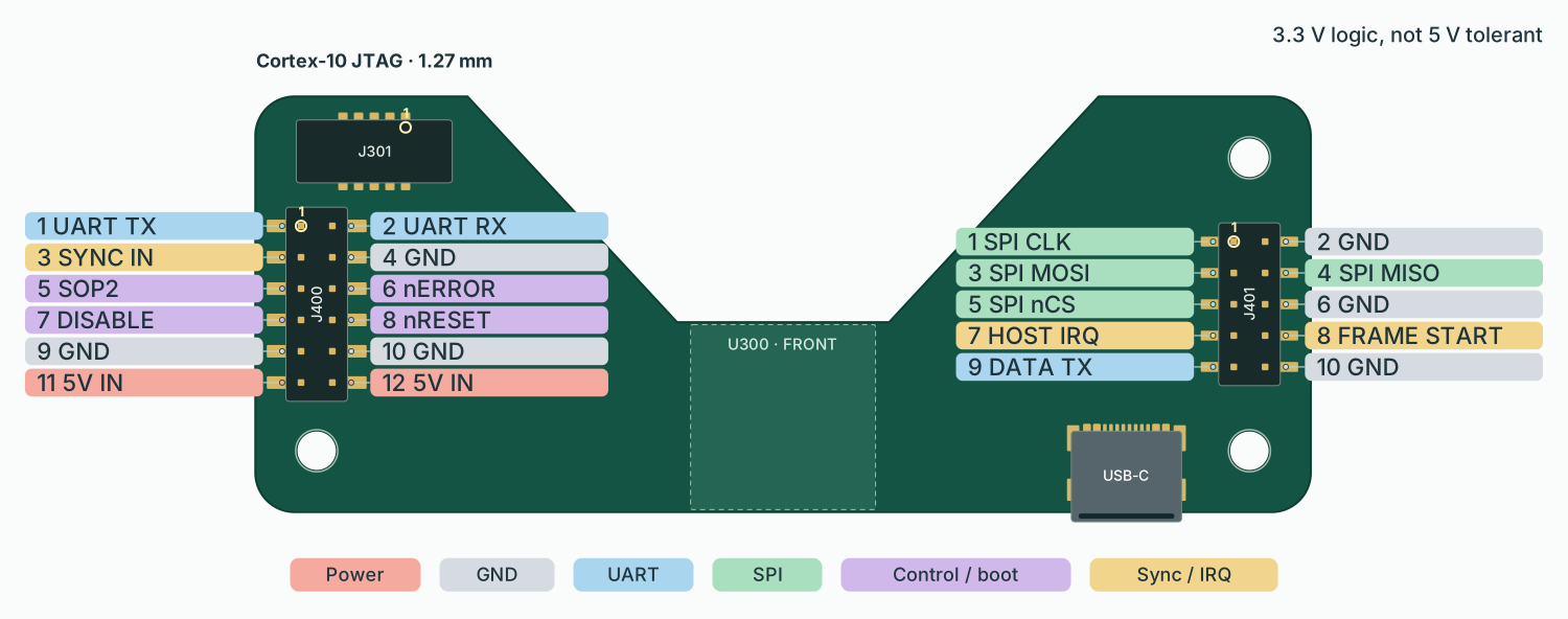
Power from one regulated 5 V supply (4.5–5.5 V, ≥ 1.5 A) on J400.11/.12, with USB unplugged. All logic is 3.3 V and not 5 V tolerant. A carrier can talk to the radar three ways:
Channel
Radar side
Pins
Direction
Use
Control UART
UARTA
TX J400.1, RX J400.2
Both
Commands, configuration, UART flashing (same UART as the USB Enhanced port)
Pull low to reset. High means rails good and reset released
HOST_DISABLE
J400.7
In, active high
High turns off every radar rail
AOP_SOP2
J400.5
In
Boot select: high during reset enters UART flashing
AOP_NERROR_OUT
J400.6
Out, open-drain
Radar error flag (optional)
HOST_SYNC_IN
J400.3
In
Frame trigger, 25 ns–4 µs pulse (optional)
FRAME_START
J401.8
Out
Frame-start pulse (optional)
To flash from a carrier: hold J400.5 high, pulse J400.8 low, program over the control UART, release J400.5 and reset again.
Carrier rules (spec §5):
Keep every carrier output and pull-up high-impedance until J400.8 first goes high, and while HOST_DISABLE is asserted.
Reset only by pulling J400.8 low open-drain; never drive it high.
Pinout
Back view: J400 is on the left and J401 on the right.
Full pin directions and carrier rules: spec §5.
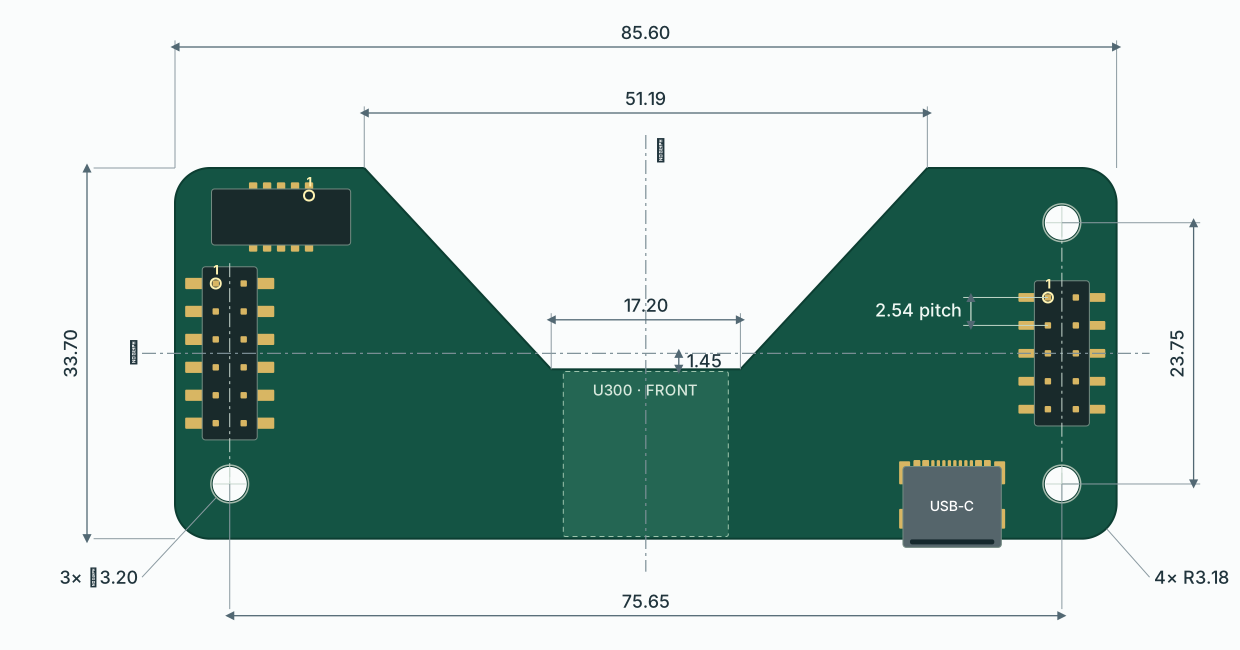
Mechanical
Back view, mm. Everything is symmetric about the board centrelines (℄). Sockets sit on the hole columns, centred vertically. Keep carrier metal out of the antenna aperture (spec §6).
Cost
First JLCPCB order, 5 boards (USD at €1 = $1.121, 5 October 2026):
5 boards
Per board
PCB
$31.85
$6.37
Assembly, including parts
$341.61
$68.32
Total
$373.46
$74.69
The IWR6843AOP is about $21 of each board. Per-part prices: docs/bom-cost.csv.
Repository layout
text
IWR-AOP-MODULE.kicad_pro / .kicad_sch / .kicad_pcb / .kicad_dru   KiCad 10 project, design rules
IWR-AOP-MODULE.kicad_sch   Power entry, LM66200 source OR, enable, integration notes
rails.kicad_sch        LP87524J-Q1 PMIC, four radar rails, reset, test pads
aop.kicad_sch          IWR6843AOP, crystal, boot flash, straps, JTAG
interfaces.kicad_sch   USB-C, CP2105 dual UART, J400 / J401 sockets, buttons
libraries/             Project symbols, footprints and STEP 3D models (IWR-AOP-MODULE.*)
                       Sockets, JTAG header, buttons and LP87524J: LCSC/EasyEDA models fitted
                       to the pads; U200: KiCad's 4x4 QFN-24 model
docs/                  Hardware specification and BOM cost
  images/              Board renders, orbit GIF, pinout.svg and dimensions.svg
  videos/              IWR-AOP-MODULE-orbit.mp4
  3d/                  Board STEP (origin: outline top-left)
tools/
  board_svg.py         Pinout and dimension SVG generation
  render/              Blender product renders and orbit video pipeline
manufacturing/         JLCPCB package builder and output (jlcpcb/)
references/            Datasheets and JLC's sample BOM format
CHANGELOG.md           Release history
LICENSE                MIT license
build/                 Generated outputs (gitignored)
The project is self-contained: everything outside the stock KiCad 10 libraries is in libraries/.
Status
In production. Revision 1.0 is fully routed. ERC is clean; DRC reports 0 unconnected and 0 schematic-parity issues, plus 36 accepted findings (spec §7.3). The bring-up checklist is spec §9.
The current product is the Panda Standard 4.7-inch parallel E0470A01-family single-board engineering design, with a replaceable 2050mAh LCO battery pack (323576) and a finished-device maximum thickness of 7mm, including…
AWR6843AOP (Antenna-on-Package) 60GHz FMCW 레이더를 이용한 존재 감지(Presence Detection) 시스템입니다. 내장 ARM Cortex-R4F MCU + C674x DSP에서 신호 처리 및 존재 판정을 수행하고, UART로 결과를 출력합니다.
Local coordinator for tado V3+ heating devices, with a Home Assistant integration and add-on
135 parts33Apache-2.0
Questions
How big is the IWR AOP MODULE PCB?
It measures 85.6 × 33.7 mm and has 6 copper layers, 1.6 mm thick.
What parts does the IWR AOP MODULE use?
158 parts, built around the IWR6843ARQGALPR, CP2105-F01-GMR, LP87524JRNFRQ1 and MX25L3233FM2I-08G. The full list of its parts is on this page, with links to each part's symbol and footprint where PCBKit's library has them.
Where can I download the IWR AOP MODULE KiCad files?
From the l3wi/IWR-AOP-MODULE repository on GitHub, at the commit this page was made from: the board is IWR-AOP-MODULE.kicad_pcb and its schematic IWR-AOP-MODULE.kicad_sch. PCBKit opens the board in the browser, with nothing to install.
Can I use the IWR AOP MODULE design in my own project?
Its repository publishes it under the MIT licence: you may reuse it on that licence's terms (keep the author's notice, and for a copyleft licence share your changes alike).