2 layers40 × 20 mm

 kripusek/krip-pad
A hack pad designed for playing some rhythm games
Pad pcb I guess is an open-source printed circuit board by kripusek, from the kripusek/krip-pad repository on GitHub. It is a 2-layer board of 143.3 × 57.9 mm with 13 parts on 18 nets, routed with 76 tracks and 2 vias.
Its parts include 4 diodes, 4 switches, 1 IC and 1 connector.
This is my macro pad madwe mainly for playing osumania type games
should be around 0.4mm
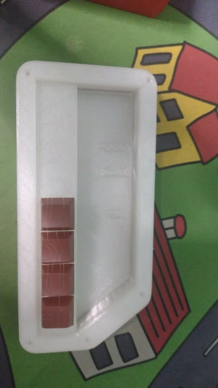 (yes I have a really cool mousepad)
Here are pictures of my pcb:
| Schematic | PCB |
|---|---|
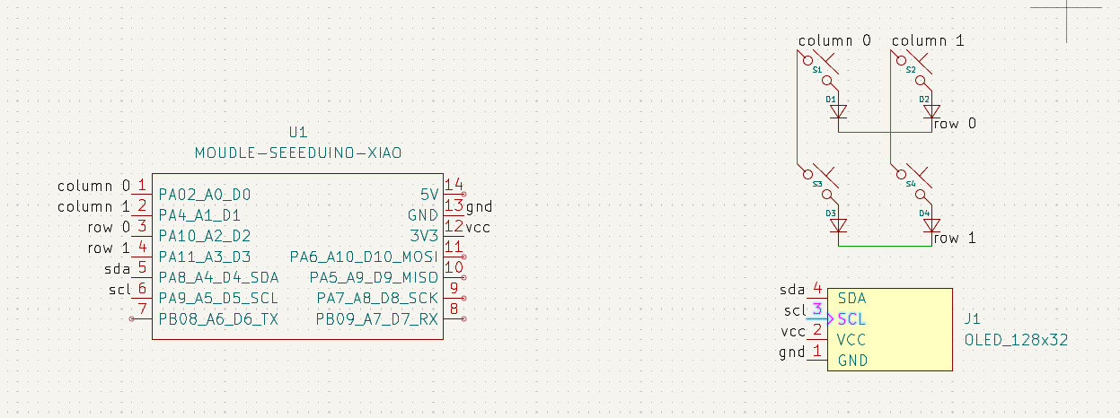 | |
I designed it using autodesk fusion
Everything fits together with 5 m3 screws and bolts
I wrote the firmware using qmk.
If you want to change the mapped you can use via with the included via.json file which you can find in the firmware folder https://usevia.app/
Making this pad was fun, I got to learn qmk fusion and kicad which I can use fluently now, fusion and qmk not so much.
I have used https://github.com/hackclub/hackpad/blob/main/hackpads/cyaopad/README.md as a template for my readme
I have used https://github.com/dancarroll/qmk-bongo for the bongo animations I have also used ai for explaining what does what in qmk, afterwards I have written the code myself and ai has helped me debug it.
| Qty | Value | Footprint | References |
|---|---|---|---|
| 4 | ~ | ScottoKeebs_MX:MX_PCB_1.00u | S1, S2, S3, S4 |
| 4 | ~ | ScottoKeebs_Components:Diode_DO-35 | D1, D2, D3, D4 |
| 3 | LOGO | LOGO | G***, G***, G*** |
| 1 | MOUDLE-SEEEDUINO-XIAO | ScottoKeebs_MCU:Seeed_XIAO_RP2040 | U1 |
| 1 | OLED_128x32 | ScottoKeebs_Components:OLED_128x32 | J1 |
It measures 143.3 × 57.9 mm and has 2 copper layers, 1.6 mm thick.
13 parts. The full list of its parts is on this page, with links to each part's symbol and footprint where PCBKit's library has them.
From the kripusek/krip-pad repository on GitHub, at the commit this page was made from: the board is pad pcb I guess/pad pcb I guess.kicad_pcb and its schematic pad pcb I guess/pad pcb I guess.kicad_sch. PCBKit opens the board in the browser, with nothing to install.
Its repository states no licence, so its author keeps all rights: ask kripusek before reusing the design.


samyk/magspoof
A portable device that can spoof/emulate any magnetic stripe, credit card or hotel card "wirelessly", even on standard magstripe (non-NFC/RFID) readers.

fossasia/pslab-scripts
Pocket Science Lab - Scripts for Sensor Experiments


willem-pennings/balancing-cube
A cube that balances itself in a corner or edge using reaction wheels

VoronDesign/Voron-Hardware
Cool Hardware designed by the Voron Design group

hoglet67/RGBtoHDMI
Bare-metal Raspberry Pi project that provides pixel-perfect sampling of Retro Computer RGB/YUV video and conversion to HDMI