4 layers24.6 × 33.1 mm

 koko69420/TP5100-Charging-Module1
Multi-cell switch-mode lithium-ion battery charging module based on TP5100 with status telemetry in KiCad
TP5100-Charging Module is an open-source printed circuit board by koko69420, from the koko69420/TP5100-Charging-Module repository on GitHub. It is a 2-layer board of 20 × 16.5 mm with 20 parts on 16 nets, routed with 126 tracks and 33 vias.
It is built around the TP5100, AO3407A and SMBJ18A. Its parts include 3 capacitors, 3 diodes, 2 connectors, 1 IC and 1 transistor. It belongs with the power boards of this library.


 [blocked]
 [blocked]
An ultra-compact, high-efficiency lithium-ion battery charging module based on the TP5100 synchronous buck switching controller, designed in KiCad with full schematic, layer plots, and 3D photorealistic visualization.
[!NOTE] Project Context (V2 Micro Redesign)
This board represents the Micro Module redesign (August 2026) of the author's original TP5100 charging board. It achieves an aggressive 66% reduction in surface area (down to just 20.0 mm × 16.5 mm) compared to the original TP5100 1S Learning Design (V1), while adding selectable 1S (4.2V) or 2S (8.4V) cell configuration, rounded corner edge cuts, and high-density double-sided SMD placement.
| Top View | Bottom View |
|---|---|
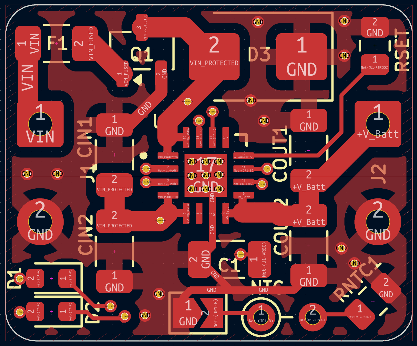 | 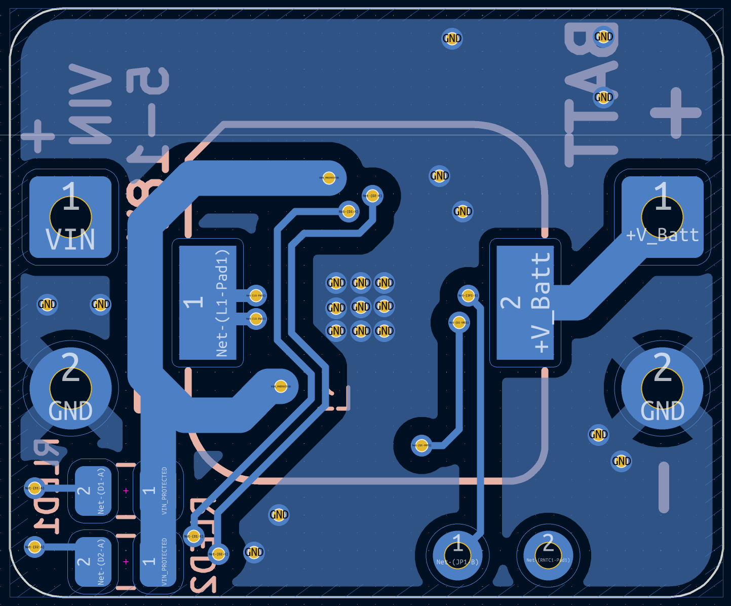 |
| Parameter | V1: KiCad Learning Board | V2: Micro Module Redesign (This Repo) |
|---|---|---|
| Role & Context | Initial design created to learn KiCad | Ultra-compact miniaturized redesign |
| Board Dimensions | 55.5 mm × 17.6 mm (977 mm²) | 20.0 mm × 16.5 mm (330 mm²) — 66% smaller |
| Edge Geometry | Standard rectangular (90° corners) | Rounded corner arcs |
| Battery Topology | 1S dedicated (4.2V) | 1S (4.2V) / 2S (8.4V) selectable via solder jumper |
| Max Charge Current | Up to 2.0 A | Up to 2.0 A |
| Input Supply | 5.0 V – 18.0 V DC | 5.0 V – 18.0 V DC |
| Component Density | Spacious layout for hand assembly | High-density double-sided SMD layout |
| Thermal Strategy | Distributed copper pours | Thermal relief via stitching under IC |
pcb.pdf, TP5100_Charging_Module-F_Cu.pdf, TP5100_Charging_Module-B_Cu.pdf).Schematic.pdf, Schematic.png).Front.png, Back.png).| Parameter | Specification | Details |
|---|---|---|
| Controller IC | TP5100 | Synchronous Step-Down Lithium Battery Charger |
| Input Supply | 5.0 V – 18.0 V DC | DC barrel jacks, USB-C 5V–12V PD, solar panels |
| Output Voltage | 4.2V (1S) / 8.4V (2S) | Solder-jumper selectable |
| Max Charge Current | 2.0 A | Current programming resistor dependent |
| Switching Freq | ~400 kHz | High-frequency operation for miniature power inductors |
| Board Dimensions | 20.0 mm × 16.5 mm | Double-sided 2-layer FR4 with rounded corners |
TP5100-Charging-Module/
├── Front.png                         # 3D PCB top surface render
├── Back.png                          # 3D PCB bottom surface render
├── Schematic.pdf                     # High-resolution vector schematic
├── Schematic.png                     # Raster schematic preview
├── pcb.pdf                           # Complete board outline and trace plots
├── TP5100_Charging_Module.kicad_sch  # KiCad schematic design file
├── TP5100_Charging_Module.kicad_pcb  # KiCad PCB board layout
├── TP5100_Charging_Module.kicad_pro  # KiCad project file
├── TP5100_Charging_Module-F_Cu.pdf   # Front copper layer plot
├── TP5100_Charging_Module-B_Cu.pdf   # Back copper layer plot
├── .gitignore                        # Git ignore patterns
└── README.md # Project documentationOpen hardware design. All rights reserved by Kausthubh Viswanath.
| Qty | Value | Footprint | References |
|---|---|---|---|
| 3 | 100 nF | Capacitor_SMD:C_1206_3216Metric | C1, CIN2, COUT2 |
| 2 | 1 kΩ | Resistor_SMD:R_0805_2012Metric | RLED1, RLED2 |
| 2 | 22 µF | Capacitor_SMD:C_1206_3216Metric | CIN1, COUT1 |
| 1 | 10 kΩ | Resistor_THT:R_Axial_DIN0204_L3.6mm_D1.6mm_P2.54mm_Vertical | NTC |
| 1 | 10 kΩ | Resistor_SMD:R_0805_2012Metric | RNTC1 |
| 1 | 3A PPTC | Fuse:Fuse_1206_3216Metric | F1 |
| 1 | AO3407A | Package_TO_SOT_SMD:SOT-23-3 | Q1 |
| 1 | Batt | Connector_Wire:SolderWire-0.5sqmm_1x02_P4.8mm_D0.9mm_OD2.3mm | J2 |
| 1 | CDRH104R | CDRH104R:CDRH104R | L1 |
| 1 | G_LED | LED_SMD:LED_0603_1608Metric | D2 |
| 1 | Input | Connector_Wire:SolderWire-0.5sqmm_1x02_P4.8mm_D0.9mm_OD2.3mm | J1 |
| 1 | R | Resistor_SMD:R_0805_2012Metric | RSET |
| 1 | R_LED | LED_SMD:LED_0603_1608Metric | D1 |
| 1 | SMBJ18A | Diode_SMD:D_SMB | D3 |
| 1 | TP5100 | TP5100:QFN65P400X400X90-17N | U1 |
| 1 | Temp Bypass | Jumper:SolderJumper-2_P1.3mm_Open_TrianglePad1.0x1.5mm | JP1 |

Circuit-Digest/Smart-Universal-Remote-with-Learning-function-and-Google-Assistant-Support
Smart Universal Remote with Learning function and Google Assistant Support

kinggh0stee/WellD
ESP32-C6 Zigbee well monitor — reads a 4–20 mA pressure transducer and DS18B20, reports water level, temperature, and battery to Zigbee2MQTT with OTA update support

SshgurkiratSingh/CCMS_PORTAL
A full-stack smart streetlight fleet management system with real-time monitoring, remote control, and analytics.

Aryan-git-byte/Soil-metrics
Portable AI-powered soil monitoring device with LTE connectivity, GPS, touchscreen interface, and real-time soil health analytics.


GrizJW/helio-485
Helio-485 KiCad board: ESP32-C5, 2S 18650, solar input, 3.3 V, 12 V 2 A, RS-485 Modbus.

It measures 20 × 16.5 mm and has 2 copper layers, 1.6 mm thick.
20 parts, built around the TP5100, AO3407A and SMBJ18A. The full list of its parts is on this page, with links to each part's symbol and footprint where PCBKit's library has them.
From the koko69420/TP5100-Charging-Module repository on GitHub, at the commit this page was made from: the board is TP5100_Charging_Module.kicad_pcb and its schematic TP5100_Charging_Module.kicad_sch. PCBKit opens the board in the browser, with nothing to install.
Its repository states no licence, so its author keeps all rights: ask koko69420 before reusing the design.