6 layers125 × 125 mm
Libreboard broken
256foundation/libreboard
Open Source Bitcoin Mining Control Board
193 parts21CERN-OHL-S-2.0

 khaydarian/spla32
SNES PPU Logic Analyzer
Spla board is an open-source printed circuit board by khaydarian, from the khaydarian/spla repository on GitHub. It is a 4-layer board of 165 × 107 mm with 290 parts on 451 nets, routed with 3,885 tracks and 710 vias.
It is built around the 74LVC1G17Z, LMH6611MK and ST1S10PHR, with the 74LVC8T245PW, 93LC66B/P and FT2232HL among its other parts. Its parts include 100 capacitors, 88 resistors, 37 ICs, 12 connectors and 10 diodes. It belongs with the sensors and measurement and retro computing and games boards and the FPGA and CPLD boards of this library.


The 1990-era Super Nintendo Entertainment System is a venerable gaming console, and although its hardware is aging and hard to come by, it has long had well-establish software emulators, preserving gaming history for generations to come.
However, while most of the SNES hardware has been effectively
reverse-engineered by writing test programs for the CPU (sometimes taking
advantage of undocumented behavior to figure out details), one remaining
component of the console has resisted complete analysis: the "Picture
Processing Unit" chips, PPU-1 and PPU-2.
The PPU chips are together responsible for managing the sprites, backgrounds, and palettes for each frame of a game's video output, and produce the analog scanline signal in realtime, which then appears on the player's TV. However, the output video signals (and video ram bus) are entirely inaccessible to SNES CPU, thus making analysis of the exact timing details of these chips difficult or impossible.
A very few games for the SNES (particularly Air Strike Patrol) use the SNES video hardware in unexpected ways, which depend on the detailed timing of the PPU chips during scanline rendering. This makes accurately emulating these games' graphics difficult -- emulator developers have to manually compare emulator output with what the game actually shows on the screen, and try to guess how the PPU evaluates these unusual configurations. Without complete understanding of the chips operation, this process degenerates into a frustruating game of whack-a-mole.
To be confident that we have faithfully reproduced the entire SNES, we need to characterize all the PPU outputs at the level of individual clock cycles, and rigorously compare the behavior of a software emulator to that of the actual, physical chips.
This project is intended to design a breakout circuit board, integrating the SNES PPU chips from a real vintage SNES console, combined with surrounding modern hardware, to effectively form a >100-pin-wide digital logic analyzer, combined with single-frame analog video capture system. With this board built, and sufficient supporting software written, it should be possible to experimentally characterize the entire operation of the PPU chips, thus producing a completely cycle-accurate emulation of the SNES video hardware.
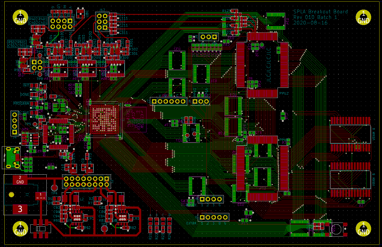
FT2232H chip, which can
drive up to 60MBps (USB 2.0 "Full Speed" maximum throughput).ECP5 FPGA, which forms the central brains of the board.PPU chips, and their corresponding video SRAM chips (which are
standard 32KiB 8-bit SRAM chips, but are old enough that they're hard to
source).74LVC8T245), as the SNES
chips are 5V TTL, but almost everything modern is 3.3V at most.ADC1173 high-speed 8-bit analog-to-digital converter chips, to
capture the analog RGB signal output and convert it back to digital for
analysis. This also requires a handful (5) of LMH6611 opamps to drive the
ADC inputs and establish reliable references.| Qty | Value | Footprint | References |
|---|---|---|---|
| 38 | 0.1uF | Capacitor_SMD:C_0603_1608Metric | C10, C11, C12, C13, C14, C15, C16, C17, C18, C19, C107, C151, C152, C207, C251, C252 +22 |
| 27 | 0 | Resistor_SMD:R_0603_1608Metric | R101, R102, R103, R108, R109, R111, R201, R202, R203, R208, R209, R211, R301, R302, R303, R308 +11 |
| 21 | 10k | Resistor_SMD:R_0603_1608Metric | R30, R31, R32, R33, R34, R35, R36, R37, R38, R39, R40, R50, R51, R52, R53, R54 +5 |
| 16 | Jumper | SPLA:BoM | BOM10, BOM11, BOM12, BOM13, BOM14, BOM15, BOM16, BOM17, BOM18, BOM19, BOM20, BOM21, BOM22, BOM23, BOM24, BOM25 |
| 15 | 0.01uF | Capacitor_SMD:C_0402_1005Metric | C20, C21, C22, C23, C24, C25, C26, C27, C28, C29, C30, C31, C32, C33, C34 |
| 15 | 74LVC8T245 | Package_SO:TSSOP-24_4.4x7.8mm_P0.65mm | U20, U21, U22, U23, U24, U25, U26, U27, U28, U29, U30, U31, U32, U33, U34 |
| 14 | NOSTUFF | Capacitor_SMD:C_0603_1608Metric | C1, C2, C101, C102, C109, C111, C201, C202, C209, C211, C301, C302, C309, C311 |
| 11 | 10uF | Capacitor_SMD:C_0603_1608Metric | C108, C153, C154, C208, C253, C254, C308, C353, C354, C408, C508 |
| 10 | LED | LED_SMD:LED_0805_2012Metric | D1, D2, D3, D4, D5, D6, D7, D8, D9, D10 |
| 9 | 330 | Resistor_SMD:R_0603_1608Metric | R20, R21, R22, R23, R24, R25, R26, R27, R28 |
| 6 | NOSTUFF | Resistor_SMD:R_0603_1608Metric | R1, R2, R3, R104, R204, R304 |
| 5 | 4.7uF | Capacitor_SMD:C_0603_1608Metric | C51, C52, C53, C83, C93 |
| 5 | LMH6611 | Package_TO_SOT_SMD:TSOT-23-6 | U61, U62, U63, U74, U75 |
| 4 | 1.65k, 1% | Resistor_SMD:R_0603_1608Metric | R121, R221, R321, R601 |
| 4 | 100pF | Capacitor_SMD:C_0603_1608Metric | C401, C402, C501, C502 |
| 4 | 10uF | Capacitor_SMD:C_0805_2012Metric | C78, C79, C81, C91 |
| 4 | 1uF | Capacitor_SMD:C_0603_1608Metric | C71, C72, C73, C74 |
| 4 | 33k | Resistor_SMD:R_0603_1608Metric | R401, R402, R501, R502 |
| 4 | Hex Standoff Female | SPLA:BoM | BOM6, BOM7, BOM8, BOM9 |
| 4 | Hex Standoff Male | SPLA:BoM | BOM2, BOM3, BOM4, BOM5 |
| 4 | MountingHole_Pad | MountingHole:MountingHole_3.2mm_M3_Pad | H1, H2, H3, H4 |
| 3 | 1k, 1% | Resistor_SMD:R_0603_1608Metric | R82, R92, R603 |
| 3 | 301, 1% | Resistor_SMD:R_0603_1608Metric | R122, R222, R322 |
| 3 | 649, 1% | Resistor_SMD:R_0603_1608Metric | R123, R223, R323 |
| 3 | ADC1173 | Package_SO:TSSOP-24_4.4x7.8mm_P0.65mm | U51, U52, U53 |
| 2 | 22uF | Capacitor_SMD:C_0805_2012Metric | C82, C92 |
| 2 | 3.3uH | Inductor_SMD:L_Vishay_IHLP-2020 | L1, L2 |
| 2 | 4.7nF | Capacitor_SMD:C_0805_2012Metric | C84, C94 |
| 2 | 74LVC1G17 | Package_TO_SOT_SMD:SOT-353_SC-70-5 | U4, U5 |
| 2 | ST1S10PHR | SPLA:ST_PowerSO-8EP_4x5mm_P1.27mm_EP3.5x2.6mm | U8, U9 |
| 1 | 100 | Resistor_SMD:R_0603_1608Metric | R5 |
| 1 | 12k, 1% | Resistor_SMD:R_0603_1608Metric | R8 |
| 1 | 2.2k | Resistor_SMD:R_0603_1608Metric | R4 |
| 1 | 3.09k, 1% | Resistor_SMD:R_0603_1608Metric | R91 |
| 1 | 3.48k, 1% | Resistor_SMD:R_0603_1608Metric | R602 |
| 1 | 4.7k | Resistor_SMD:R_0402_1005Metric | R6 |
| 1 | 5.23k, 1% | Resistor_SMD:R_0603_1608Metric | R81 |
| 1 | 56pF | Capacitor_SMD:C_0603_1608Metric | C49 |
| 1 | 750 | Resistor_SMD:R_0603_1608Metric | R7 |
| 1 | 93LC66B | Package_SO:SOIC-8_3.9x4.9mm_P1.27mm | U3 |
| 1 | Barrel_Jack | Connector_BarrelJack:BarrelJack_CUI_PJ-036AH-SMT_Horizontal | J1 |
| 1 | FT2232H | Package_QFP:LQFP-64_10x10mm_P0.5mm | U2 |
| 1 | FT5HNBPK12.0-T1 | Crystal:Crystal_SMD_5032-4Pin_5.0x3.2mm | X1 |
| 1 | JS202011SCQN | SPLA:JS202011SCQN | SW2 |
| 1 | J_ANALOG | Connector_PinHeader_2.54mm:PinHeader_2x03_P2.54mm_Vertical | J12 |
| 1 | J_AREF | Connector_PinHeader_2.54mm:PinHeader_2x04_P2.54mm_Vertical | J10 |
| 1 | J_AREF_AMP | Connector_PinHeader_2.54mm:PinHeader_2x02_P2.54mm_Vertical | J11 |
| 1 | J_BODGE | Connector_PinHeader_2.54mm:PinHeader_1x04_P2.54mm_Vertical | J6 |
| 1 | J_DPULL | Connector_PinHeader_2.54mm:PinHeader_1x03_P2.54mm_Vertical | J9 |
| 1 | J_EXTRA | Connector_PinHeader_2.54mm:PinHeader_1x05_P2.54mm_Vertical | J5 |
| 1 | J_JTAG | Connector_PinHeader_2.54mm:PinHeader_1x04_P2.54mm_Vertical | J4 |
| 1 | J_POWER | Connector_PinHeader_2.54mm:PinHeader_2x08_P2.54mm_Vertical | J2 |
| 1 | J_PPURESET | Connector_PinHeader_2.54mm:PinHeader_1x03_P2.54mm_Vertical | J8 |
| 1 | J_SAMPLE | Connector_PinHeader_2.54mm:PinHeader_1x06_P2.54mm_Vertical | J7 |
| 1 | LFE5U-45F-BG256 | Package_BGA:BGA-256_14.0x14.0mm_Layout16x16_P0.8mm_Ball0.45mm_Pad0.32mm_NSMD | U1 |
| 1 | PTS645 | SPLA:PTS645-SMTR92 | SW1 |
| 1 | SNES_PPU1 | SPLA:QFP-100_14x20mm_P0.65mm | U10 |
| 1 | SNES_PPU2 | SPLA:QFP-100_14x20mm_P0.65mm | U11 |
| 1 | TLV73311PDBV | Package_TO_SOT_SMD:SOT-23-5 | U7 |
| 1 | TLV73325PDBV | Package_TO_SOT_SMD:SOT-23-5 | U6 |
| 1 | TLV73333PDBV | Package_TO_SOT_SMD:SOT-23-5 | U80 |
| 1 | TP_12MHZ | TestPoint:TestPoint_Pad_D1.0mm | TP6 |
| 1 | TP_12V | TestPoint:TestPoint_Pad_D2.0mm | TP3 |
| 1 | TP_1V8 | TestPoint:TestPoint_Pad_D1.0mm | TP5 |
| 1 | TP_AREF_HI | TestPoint:TestPoint_Pad_D1.0mm | TP7 |
| 1 | TP_AREF_LO | TestPoint:TestPoint_Pad_D1.0mm | TP8 |
| 1 | TP_AVCC | TestPoint:TestPoint_Pad_D1.0mm | TP9 |
| 1 | TP_FPGA_XIN | TestPoint:TestPoint_Pad_D1.0mm | TP1 |
| 1 | TP_GND | TestPoint:TestPoint_Pad_D2.0mm | TP4 |
| 1 | TP_TAP_XIN | TestPoint:TestPoint_Pad_D1.0mm | TP2 |
| 1 | USB Cable | SPLA:BoM | BOM1 |
| 1 | USB_B_Micro | Connector_USB:USB_Micro-B_Wuerth_629105150521 | J3 |
| 1 | VRAM_A | SPLA:SOP-28_17x8mm_P1.27mm | U12 |
| 1 | VRAM_B | SPLA:SOP-28_17x8mm_P1.27mm | U13 |
It measures 165 × 107 mm and has 4 copper layers, 1.6 mm thick.
290 parts, built around the 74LVC1G17Z, LMH6611MK, ST1S10PHR and 74LVC8T245PW. The full list of its parts is on this page, with links to each part's symbol and footprint where PCBKit's library has them.
From the khaydarian/spla repository on GitHub, at the commit this page was made from: the board is spla-board/spla-board.kicad_pcb. PCBKit opens the board in the browser, with nothing to install.
Its repository states no licence, so its author keeps all rights: ask khaydarian before reusing the design.
256foundation/libreboard
Open Source Bitcoin Mining Control Board

tsar-boomba/dap-proto-board-full
The culmination of all of my learning during the Spring '26 semester. All the way from making a simple dev board for the TAD5212 DAC, to making a RP2350 board, and now this. Everything combined on one 6-layer board.

supermomo31/PCE_colorlight_carrier
console PCE depuis un FPGA format SODIMM : colorlight i5


RubenVoell/iceduino
The basic idea behind this project is to create a simple breakout of an ICE40 FPGA with some LEDs and Buttons to interact with the FPGA and enough resources to run a simple softcore, like a small RISC-V core.


CK20000/Isolated-Half-Bridge-Driver
An isolated half-bridge motor driver board featuring 6N137 galvanic protection, an IR2101 bootstrap topology, and precise AD8418 bidirectional current sensing.
