2 layers50 × 100 mm

 kbranch/snowflake_keyboard3
A weird, tightly spaced split keyboard
Snowflake is an open-source printed circuit board by kbranch, from the kbranch/snowflake_keyboard repository on GitHub, published under the MIT licence. It is a 2-layer board of 149.8 × 96.3 mm with 114 parts on 78 nets, routed with 956 tracks and 117 vias.
It is built around the ATMEGA32U4RC-AU and SK6805E-J. Its parts include 36 diodes, 14 capacitors, 5 resistors, 3 ICs and 1 switch. It belongs with the keyboards and input boards and the AVR (ATmega, ATtiny) boards of this library.


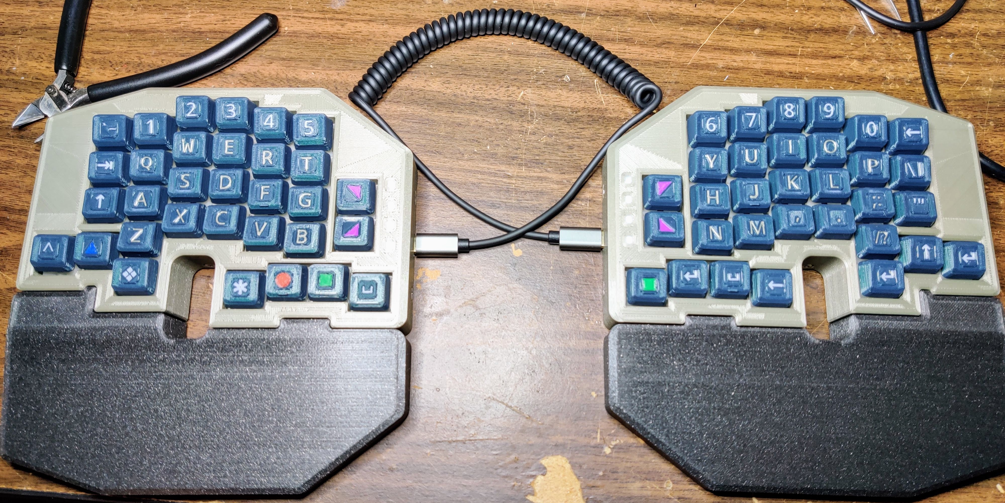
This is a weird, tightly spaced split keyboard that I designed to be very specific to my needs. It uses 17x16 mm key spacing rather than the standard 19x19 mm (inspired by this post). The odd keys on the outside bottom corners are meant to be pressed with the pinky's knuckle rather than a fingertip. I haven't included every detail necessary to build the whole keyboard since it's so specific to my needs, but I'm happy to share and/or answer questions if somebody is interested in more detail for some reason.
The original CAD files are public on OnShape: Case and Keycaps. Generating the keycap legends is a pretty manual and sometimes fiddly process. I believe I included copies of all of the STLs I used, but I may have forgotten a few. 3mf files are included for the keycaps and legends, which should load into PrusaSlicer with all models in their correct quantities and print settings ready to go for a Prusa i3 MK3S.
All 3D printed parts are designed to be printed without support. I used manual mid-print color changes to embed the LED diffuser pieces into the case and for the keycap legends. M2 screws and nuts hold the PCB and plate to the case, and M3 screws and nuts hold the case halves and palm rests together. Little o-rings sit between the plate and case.
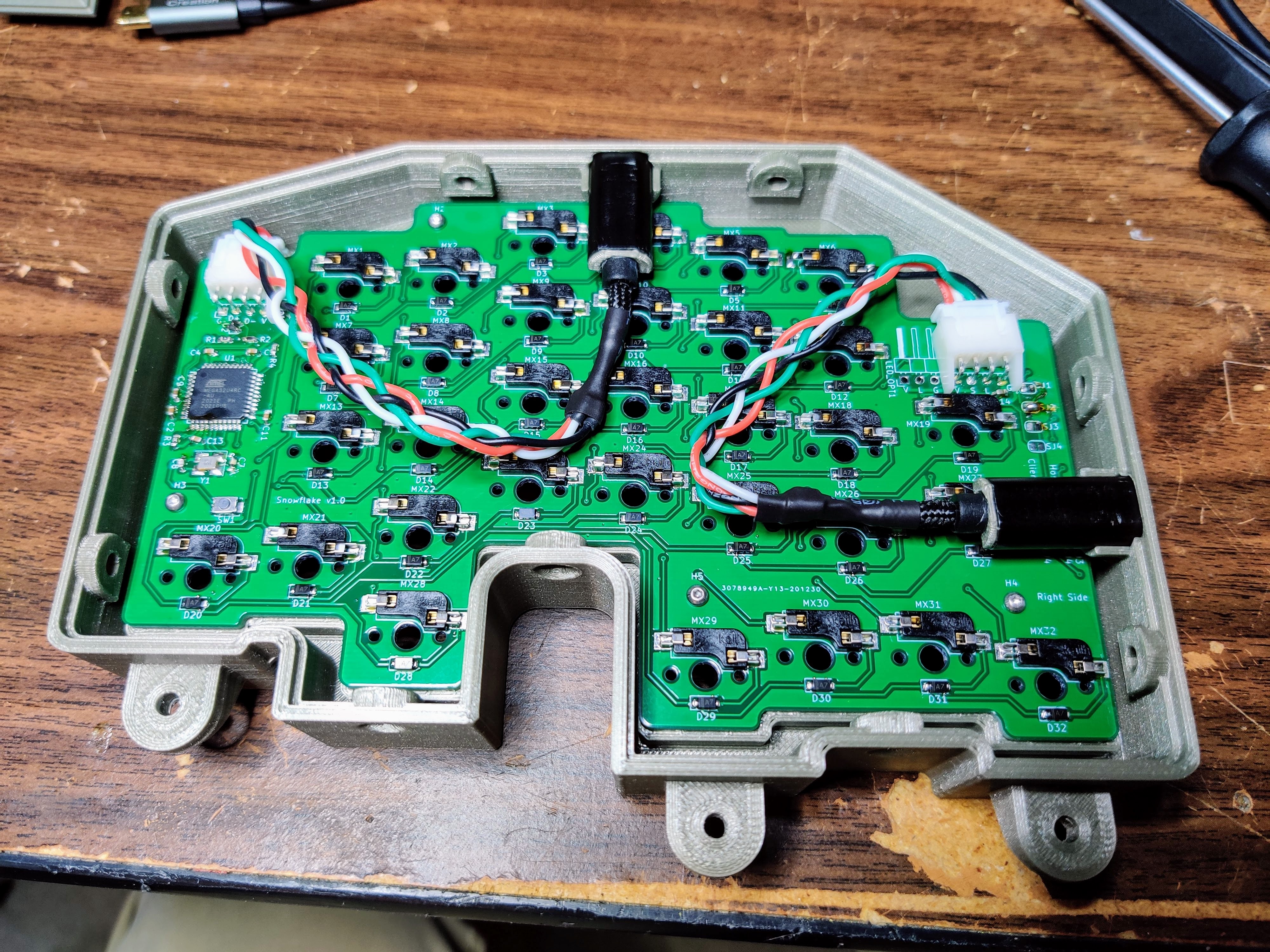
I used USB-C for both the actual USB connector and the board to board connection. I repurposed some USB-A to USB-C adapters to use as panel mount USB-C connectors. I ended up needing to grind the fronts down a bit to allow for cables to snap in fully through the case thickness.
The referenced QMK version includes a small tweak to allow the brightness of the indicator LEDs to follow the regular LED animation brightness. The LEDs are set up to indicate the active layer and the status of num, caps and scroll lock - they're not intended for flashy animations.
| Qty | Value | Footprint | References |
|---|---|---|---|
| 32 | D | Diode_SMD:D_SOD-123 | D1, D2, D10, D11, D12, D13, D14, D15, D16, D17, D18, D19, D20, D21, D22, D23 +16 |
| 32 | MX-NoLED | keyswitches:Kailh_socket_MX | MX1, MX2, MX10, MX11, MX12, MX13, MX14, MX15, MX16, MX17, MX18, MX19, MX20, MX21, MX22, MX23 +16 |
| 9 | 0.1uf | Capacitor_SMD:C_0603_1608Metric_Pad1.08x0.95mm_HandSolder | C2, C3, C4, C5, C6, C10, C11, C12, C13 |
| 8 | , , , , , , , | ||
| 5 | MountingHole | MountingHole:MountingHole_2.2mm_M2 | H1, H2, H3, H4, H5 |
| 4 | SK6805 | LED_SMD:LED_SK6805_PLCC4_2.4x2.7mm_P1.3mm | D33, D34, D35, D36 |
| 4 | SolderJumper | Jumper:SolderJumper-2_P1.3mm_Open_RoundedPad1.0x1.5mm | SJ1, SJ2, SJ3, SJ4 |
| 2 | footprints:TPD2E2U06DCKR | U2, U3 | |
| 2 | 10k | Resistor_SMD:R_0603_1608Metric_Pad0.98x0.95mm_HandSolder | R3, R4 |
| 2 | 10uf | Capacitor_SMD:C_0603_1608Metric_Pad1.08x0.95mm_HandSolder | C1, C14 |
| 2 | 22 | Resistor_SMD:R_0603_1608Metric_Pad0.98x0.95mm_HandSolder | R1, R2 |
| 2 | 22pf | Capacitor_SMD:C_0603_1608Metric_Pad1.08x0.95mm_HandSolder | C7, C8 |
| 1 | 16MHz | Crystal:Crystal_SMD_3225-4Pin_3.2x2.5mm_HandSoldering | Y1 |
| 1 | 1uf | Capacitor_SMD:C_0603_1608Metric_Pad1.08x0.95mm_HandSolder | C9 |
| 1 | 470 | Resistor_SMD:R_0603_1608Metric_Pad0.98x0.95mm_HandSolder | R5 |
| 1 | 500ma | Fuse:Fuse_0805_2012Metric_Castellated | F1 |
| 1 | ATmega32U4RC-AU | Package_QFP:TQFP-44_10x10mm_P0.8mm | U1 |
| 1 | AVR-ISP-6 | Connector_PinHeader_2.54mm:PinHeader_2x03_P2.54mm_Vertical | ISP |
| 1 | LED | Connector_PinHeader_2.54mm:PinHeader_1x03_P2.54mm_Horizontal | LED_OPT1 |
| 1 | SPLIT | Connector_PinHeader_2.54mm:PinHeader_1x04_P2.54mm_Horizontal | SPLIT1 |
| 1 | SW_Push | Button_Switch_SMD:SW_Push_SPST_NO_Alps_SKRK | SW1 |
| 1 | USB | Connector_PinHeader_2.54mm:PinHeader_1x04_P2.54mm_Horizontal | USB1 |
It measures 149.8 × 96.3 mm and has 2 copper layers, 1.6 mm thick.
114 parts, built around the ATMEGA32U4RC-AU and SK6805E-J. The full list of its parts is on this page, with links to each part's symbol and footprint where PCBKit's library has them.
From the kbranch/snowflake_keyboard repository on GitHub, at the commit this page was made from: the board is pcb_files/snowflake.kicad_pcb. PCBKit opens the board in the browser, with nothing to install.
Its repository publishes it under the MIT licence: you may reuse it on that licence's terms (keep the author's notice, and for a copyleft licence share your changes alike).

ea4gge/A500Mini-Internal-Functional-Keyboard
This is the Ongoing project of the A500Mini internal functional keyboard based in 32U4 processor (Arduino leonardo, for example).


Marco-Antonio-Mares-Mejia/Proyecto-NumPad
Proyecto de diseño de un pad numérico simple.

yycho0108/Eclectronics-Project-3
Project 3 : Indoor Localization System for ENGR3430: Eclectronics

ParadigmHyperloop/electrical
All schematics and layouts in KiCad, plus some simulations

reivax-boucoi/PCB_Kicad
Repo for all my home projects involving PCBs developped with Kicad
