

4 layers21.7 × 89.8 mm

 Karthikeya2005/buck5v
A 2-layer synchronous buck converter board built around the Texas Instruments TPS54202. Input is 9 to 24 V, output is 5 V at up to 2 A, with a switching frequency of about 500 kHz.
Buck5v is an open-source printed circuit board by Karthikeya2005, from the Karthikeya2005/buck5v repository on GitHub, published under the MIT licence. It is a 2-layer board of 45 × 35 mm with 20 parts on 8 nets, routed with 38 tracks and 50 vias.
It is built around the TPS54202DDCR and SS34. Its parts include 7 capacitors, 4 resistors, 2 connectors, 1 IC and 1 diode.
A 2-layer synchronous buck converter board built around the Texas Instruments TPS54202. Input is 9 to 24 V, output is 5 V at up to 2 A, with a switching frequency of about 500 kHz.
Status: designed and checked in software only. The board has not been fabricated, assembled or measured. Every figure below is a calculation from the datasheet, not a bench result. Part sourcing (stock, LCSC numbers) was not verified either.
I built this to learn power-supply design end to end: choosing the IC, calculating each component, wiring the schematic, laying out the board around the switching loop, and checking it with ERC and DRC. I checked the datasheet values and reviewed the schematic, layout and DRC results myself.
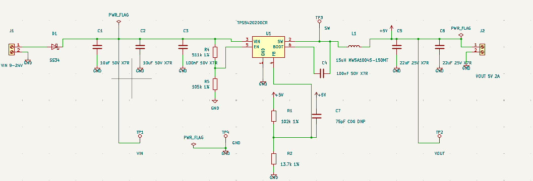
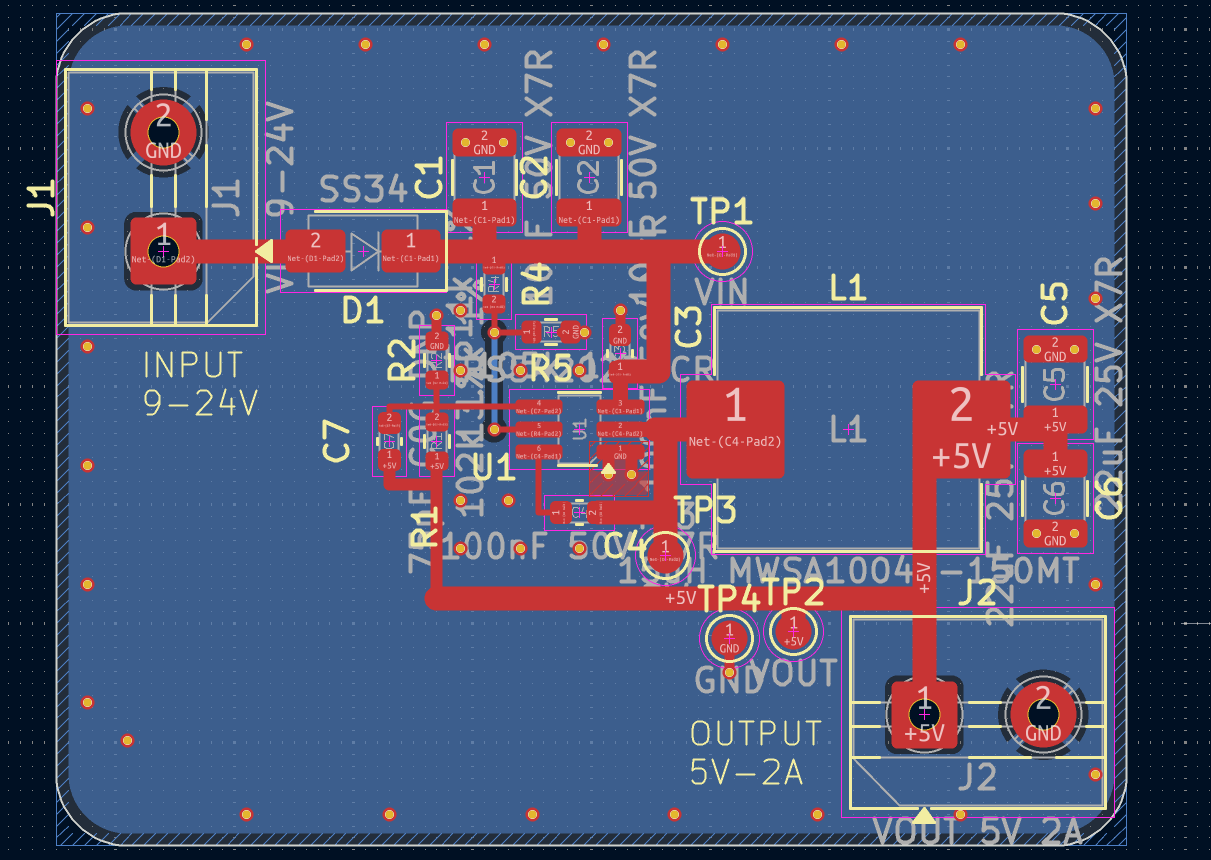
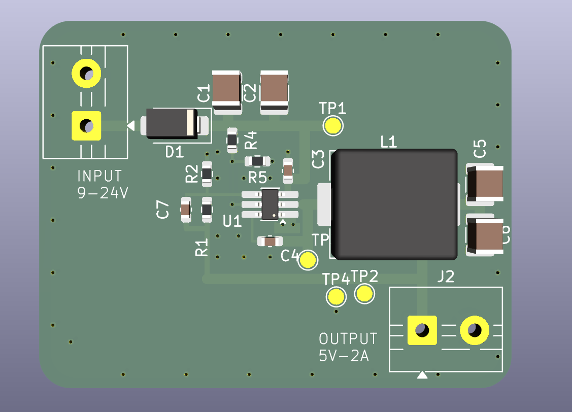
| Parameter | Value |
|---|---|
| Input voltage | 9 to 24 V (IC accepts 4.5 to 28 V) |
| Output voltage | 5 V (about 5.03 V typical) |
| Output current | 2 A |
| Switching frequency | 500 kHz typical (390 to 630 kHz) |
| Topology | Synchronous buck, integrated FETs |
| Board | 2 layers, 45 x 35 mm |
| Protection | Series Schottky for reverse polarity, EN divider as undervoltage lockout |
4.5 to 28 V input, 2 A, internal high-side and low-side FETs, so no external catch diode is needed. Datasheet values I used: feedback voltage VFB = 0.596 V (0.581 to 0.611 V), switching frequency 500 kHz, low-side current limit up to 4.3 A.
Vout = VFB x (1 + R1 / R2) = 0.596 x (1 + 102 k / 13.7 k) = 5.03 V typical. Over the VFB tolerance the output spans 4.91 to 5.16 V. Both resistors are standard 1% values.
L = 15 uH (Sunlord MWSA1004S-150MT: 45 mOhm DCR max, Isat 5.6 A taken conservatively from the datasheet).
| Vin | Duty cycle | Ripple current (p-p) | Peak current at 2 A load |
|---|---|---|---|
| 9 V | 0.56 | 0.30 A | 2.15 A |
| 12 V | 0.42 | 0.39 A | 2.19 A |
| 24 V | 0.21 | 0.53 A | 2.26 A |
Ripple current = Vout x (1 - D) / (L x f). Peak current stays well below both the inductor's 5.6 A saturation current and the IC's 4.3 A maximum low-side limit.
| Ref | Value | Role |
|---|---|---|
| C1, C2 | 10 uF 50 V X7R (1210) | Bulk input |
| C3 | 100 nF 50 V X7R (0603) | High-frequency input decoupling, placed at the VIN pin |
| C4 | 100 nF 50 V X7R (0603) | Bootstrap, BOOT to SW |
| C5, C6 | 22 uF 25 V X7R (1210) | Output |
| C7 | 75 pF C0G (0603), not populated | Optional feed-forward across R1 |
Ceramic capacitance falls with DC bias, so the effective output capacitance at 5 V is lower than 44 uF. Output ripple depends mostly on ESR and layout, so it has to be measured on a real board.
R4 = 511 k from VIN to EN, R5 = 105 k from EN to GND. With the datasheet EN rising threshold of 1.21 V typical (1.28 V max), the converter starts at about 7.1 V (7.5 V worst case) at the IC's VIN node. EN sees about 1.5 V at 9 V in and about 4.1 V at 24 V in. Check this against the datasheet's absolute maximum rating for EN before building.
D1 is an SS34 Schottky in series with the input. It costs roughly 0.5 V and about 0.6 W at 9 V in and 2 A out. A P-channel MOSFET would waste less power but needs extra parts.
| Ref | Value | Footprint |
|---|---|---|
| U1 | TPS54202DDCR | TSOT-23-6 (hand-solder variant) |
| L1 | 15 uH, MWSA1004S-150MT | Sunlord MWSA1004S |
| D1 | SS34 Schottky | SMA |
| C1, C2 | 10 uF 50 V X7R | 1210 |
| C3, C4 | 100 nF 50 V X7R | 0603 |
| C5, C6 | 22 uF 25 V X7R | 1210 |
| C7 | 75 pF C0G (DNP) | 0603 |
| R1 | 102 k 1% | 0603 |
| R2 | 13.7 k 1% | 0603 |
| R4 | 511 k 1% | 0603 |
| R5 | 105 k 1% | 0603 |
| J1, J2 | 2-pin screw terminal | 5.00 mm pitch |
| TP1 to TP4 | Test points: VIN, VOUT, SW, GND | 1.5 mm pad |
Ordering would need a fresh sourcing pass. Several part numbers (including the inductor) were not confirmed in stock, and the 5.00 mm terminal block should be matched to a real part.
| Check | Result |
|---|---|
| ERC | 0 errors (PWR_FLAG symbols added to VIN, GND and +5V) |
| DRC | 0 errors, 0 unconnected items at the last run |
| DRC warnings | Mostly stitching vias flagged "not connected on one layer" (the top-layer GND zone only covers a small patch near the IC) and a few silkscreen overlaps |
| Schematic to board sync | No differences |
| Test | Setup | What to look for |
|---|---|---|
| Power-up | Bench supply at 12 V, current limit 0.2 A, no load | 5.0 V on TP2, no oscillation or smoke |
| Output accuracy | 9, 12, 24 V in, no load and 2 A load | Output within about +/-3% of 5 V |
| Efficiency | 0.1, 0.25, 0.5, 1, 1.5, 2 A at 9, 12, 24 V | Measure Vin and Iin at the board terminals, Vout and Iout at the load |
| Output ripple | Scope on TP2 with spring ground at TP4, 20 MHz bandwidth | Ripple in mV, compare with the estimate |
| SW waveform | Scope on TP3 | Duty cycle, ringing, frequency near 500 kHz |
| Load step | 0.2 A to 2 A | Overshoot and recovery |
| Thermal | 2 A for 10 minutes, thermal camera or thermocouple | IC and inductor temperature rise |
| Start-up threshold | Slowly raise Vin from 0 | Converter starts near 7 to 7.6 V |
buck5v.kicad_pro        KiCad project
buck5v.kicad_sch        Schematic
buck5v.kicad_pcb        PCB layout
buck5v.kicad_sym        Project symbol library (TPS54202)
sym-lib-table           Library table for the project symbol
docs/                   Images of the schematic, board and 3D view
fab/                    Gerber files, drill files and BOM (CSV)
buck5v-gerbers.zip      The fab/ folder zipped, ready to upload to a board house
Open buck5v.kicad_pro in KiCad 10 or newer.
KiCad 10. Datasheet values were checked by hand against the TI TPS54202 and Sunlord MWSA-S datasheets.
MIT. See LICENSE. There is no warranty, and nobody has independently reviewed this design. Have it reviewed before building it or using it in anything that matters.
| Qty | Value | Footprint | References |
|---|---|---|---|
| 2 | 100nF 50V X7R | Capacitor_SMD:C_0603_1608Metric | C3, C4 |
| 2 | 10uF 50V X7R | Capacitor_SMD:C_1210_3225Metric | C1, C2 |
| 2 | 22uF 25V X7R | Capacitor_SMD:C_1210_3225Metric | C5, C6 |
| 1 | 102k 1% | Resistor_SMD:R_0603_1608Metric | R1 |
| 1 | 105k 1% | Resistor_SMD:R_0603_1608Metric | R5 |
| 1 | 13.7k 1% | Resistor_SMD:R_0603_1608Metric | R2 |
| 1 | 15uH MWSA1004S-150MT | Inductor_SMD:L_Sunlord_MWSA1004S | L1 |
| 1 | 511k 1% | Resistor_SMD:R_0603_1608Metric | R4 |
| 1 | 75pF C0G DNP | Capacitor_SMD:C_0603_1608Metric | C7 |
| 1 | GND | TestPoint:TestPoint_Pad_D1.5mm | TP4 |
| 1 | SS34 | Diode_SMD:D_SMA | D1 |
| 1 | SW | TestPoint:TestPoint_Pad_D1.5mm | TP3 |
| 1 | TPS54202DDCR | Package_TO_SOT_SMD:TSOT-23-6_HandSoldering | U1 |
| 1 | VIN | TestPoint:TestPoint_Pad_D1.5mm | TP1 |
| 1 | VIN 9-24V | TerminalBlock:TerminalBlock_MaiXu_MX126-5.0-02P_1x02_P5.00mm | J1 |
| 1 | VOUT | TestPoint:TestPoint_Pad_D1.5mm | TP2 |
| 1 | VOUT 5V 2A | TerminalBlock:TerminalBlock_MaiXu_MX126-5.0-02P_1x02_P5.00mm | J2 |


vkar9898/Cluster2HDMI
A project dedicated to utilising a 7 inch LCD panel as a standalone monitor via a HDMI-parallel RGB converter and a Pico 2 fitted on a custom PCB


ColumbiaGadgetWorks/cardboard-bot-v2
60 × 46 mm, 2-layer, 2 oz copper, for a 2S or 3S LiPo on a screw terminal. JLCPCB assembles the SMD parts on the top side; CGW hand-solders the through-hole parts. Nothing goes on the back.


Miroeilola/vallox-rs485-controller
Replacement control panel for legacy Vallox SE ventilation units. Vallox DIGIT RS-485 protocol, bus-powered, ESP32, Home Assistant.

EmanresuEmanreztuneb/SimpleFOC_G431_Motordriver
A motordriver based in STM's G431 Drone ESC.
It measures 45 × 35 mm and has 2 copper layers, 1.6 mm thick.
20 parts, built around the TPS54202DDCR and SS34. The full list of its parts is on this page, with links to each part's symbol and footprint where PCBKit's library has them.
From the Karthikeya2005/buck5v repository on GitHub, at the commit this page was made from: the board is buck5v.kicad_pcb and its schematic buck5v.kicad_sch. PCBKit opens the board in the browser, with nothing to install.
Its repository publishes it under the MIT licence: you may reuse it on that licence's terms (keep the author's notice, and for a copyleft licence share your changes alike).