2 layers
Nrf bga
github-linguist/linguist
Language Savant. If your repository's language is being reported incorrectly, send us a pull request!
12 parts14kMIT

 Karpova-Lab/camera-link3
Link between pyControl and Chameleon3 USB3 camera
Camera link is an open-source printed circuit board by Karpova-Lab, from the Karpova-Lab/camera-link repository on GitHub. It is a 2-layer board of 189.2 × 19 mm with 12 parts on 15 nets, routed with 55 tracks and 2 vias.
It is built around the E5J88-00LJG2-L. Its parts include 3 diodes, 2 connectors and 1 resistor.
This PCB connects a Chameleon3 USB3 camera to pyControl. It takes "frame grab" and "sync pulse" signals generated by pyControl and coming out of a D-Series Breakout Board and routes them into the GPIO pins of the camera.
Additionally, the PCB has 3 controllable high power IR LEDs that provide light for the camera to see in the dark.



| Qty | Reference | Description | Value/MPN |
|---|---|---|---|
| 3 | D1, D2, D3 | 850 nm LED | LST1-01F09-IR01-00 |
| 2 | H1, H2 | Threaded standoff | 24882 |
| 1 | J1 | 9-pin socket | BM09B-NSHSS-TBT |
| 1 | J2 | RJ45 jack | E5J88-00LJG2-L |
| 1 | R1 | 5 watt resistor | 5Ω |
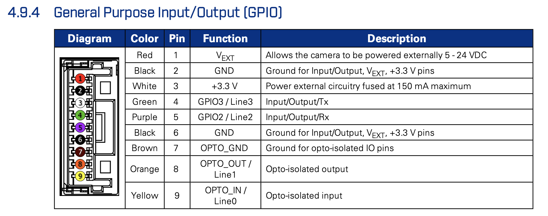
| GPIO pin | GPIO Color | GPIO Function | RJ45 Pin | pyControl Function | Purpose |
|---|---|---|---|---|---|
| 4 | Green | GPIO3/Line3 | 1 | DIO_A | pyControl sends square wave to camera to grab each frame |
| 9 | Yellow | OPTO_IN/Line0 | 4 | DIO_B | pyControl sends random sync pulse |
| 6 | Black | GND | 2 | Ground | Ground |
| 7 | Brown | OPTO_GND | 2 | Ground | Ground |
| Qty | Value | Footprint | References |
|---|---|---|---|
| 4 | TestPoint | Connector_Pin:Pin_D1.0mm_L10.0mm | GND1, GND2, GRAB1, SYNC1 |
| 3 | LST1-01F09-IR01-00 | asl_footprints:LED_starboard | D1, D2, D3 |
| 2 | 24882 | asl_footprints:standoff_nut | H1, H2 |
| 1 | 5Ω | Resistor_THT:R_Axial_DIN0614_L14.3mm_D5.7mm_P7.62mm_Vertical | R1 |
| 1 | Conn_01x09_Female | asl_footprints:JST_NSH_1x09_VERTICAL | J1 |
| 1 | E5J88-00LJG2-L | asl_footprints:RJ45_THP_tab_on_top | J2 |
It measures 189.2 × 19 mm and has 2 copper layers, 1.6 mm thick.
12 parts, built around the E5J88-00LJG2-L. The full list of its parts is on this page, with links to each part's symbol and footprint where PCBKit's library has them.
From the Karpova-Lab/camera-link repository on GitHub, at the commit this page was made from: the board is pcb/camera_link.kicad_pcb and its schematic pcb/camera_link.kicad_sch. PCBKit opens the board in the browser, with nothing to install.
Its repository states no licence, so its author keeps all rights: ask Karpova-Lab before reusing the design.
github-linguist/linguist
Language Savant. If your repository's language is being reported incorrectly, send us a pull request!


google/mozc-devices
Circuit diagrams and firmware source code for Gboard DIY keyboards


hackclub/OnBoard
💡 Join 1,000 teenagers and make your first PCB with a $100 grant!

VoronDesign/Voron-Tap
Tap is a nozzle-based z-probe for the V2 and Trident printer designs. The entire toolhead moves to trigger an optical switch. Tap offers many advantages:

stacksmashing/pico-tpmsniffer
A simple, very experimental TPM sniffer for LPC bus