

2 layers75.7 × 28 mm
PRISM
Gusus169/PRISM-The-usb-hub
A compact 4-port USB 2.0 hub PCB featuring ESD protection, PTC resettable fuses, and per-port LED indicators.
46 partsMIT

 karhincheong/EgHub
PCB Keychain for Hackclub Fallout
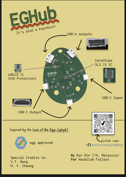
USB HUB is an open-source printed circuit board by karhincheong, from the karhincheong/EgHub repository on GitHub, published under the GPL-3.0 licence. It is a 2-layer board of 66.5 × 89.2 mm with 33 parts on 27 nets, routed with 267 tracks and 42 vias.
It is built around the SL2.1S and USBLC6-2SC6. Its parts include 16 capacitors, 6 resistors and 6 ICs. It belongs with the interfaces and adapters boards of this library.
A 4-port output USB Hub keychain in the shape of an egg as a tribute to my friends. Main IC being CoreChips SL2.1S
This project is meant to be a try-out project for Fallout. It is to function as a primer for me to learn to make/design a PCB and at the same time make something useful.
| Item | Description | Quantity | Unit Price (USD) | Total Price (USD) | URL | Notes |
|---|---|---|---|---|---|---|
| Capacitor | 0805 1 uF | 16 | 0.0469 | 0.94 | https://www.lcsc.com/product-detail/C28323.html | MOQ=20 |
| 0805 100 nF | 16 | 0.0133 | 1.33 | https://www.lcsc.com/product-detail/C49678.html | MOQ=100 | |
| Resistor | 0805 5.1 kΩ | 12 | 0.0028 | 0.28 | https://www.lcsc.com/product-detail/C27834.html | MOQ=100 |
| USB-A Receptacle | 4 | 0.0665 | 0.67 | https://www.lcsc.com/product-detail/C668591.html | MOQ=10 | |
| USB-C Receptacle | 6 | 0.0741 | 1.48 | https://www.lcsc.com/product-detail/C2765186.html | MOQ=20 | |
| CoreChips SL2.1S | 2 | 0.2849 | 1.42 | https://www.lcsc.com/product-detail/C2684433.html | MOQ=5 | |
| USBLC6-2SC6 | 16 | 0.154 | 3.08 | https://www.lcsc.com/product-detail/C7519.html | MOQ=20 | |
| PCB (JLCPCB) Order | 1 | 2.0000 | 2.00 | https://www.jlcpcb.com | MOQ=5 | |
| TOTAL (for 2 units) | 11.20 | |||||
| Component Cost per Unit | 5.60 |
| Item | Description | Price (USD) |
|---|---|---|
| Shipping | UPS Worldwide Express Saver | 9.24 |
File System
| Folder | Description |
|---|---|
kicad/ | Files generated in KiCAD |
3d/ | 3D Mechanical Models for the case and the PCB |
gerbers/ | Gerber Files |
production/ | Production files for manufacturers |
You may choose to hand solder the components onto the PCB.
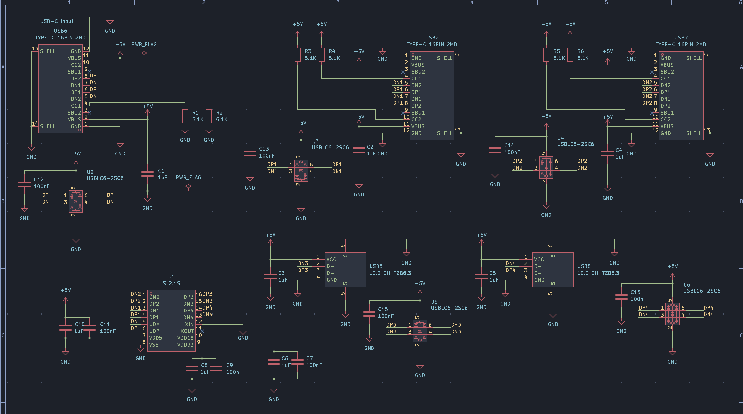
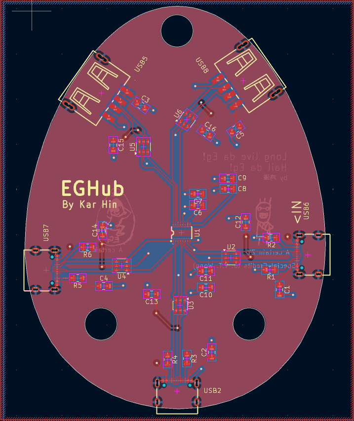
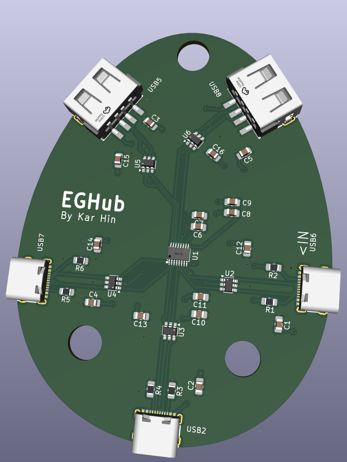
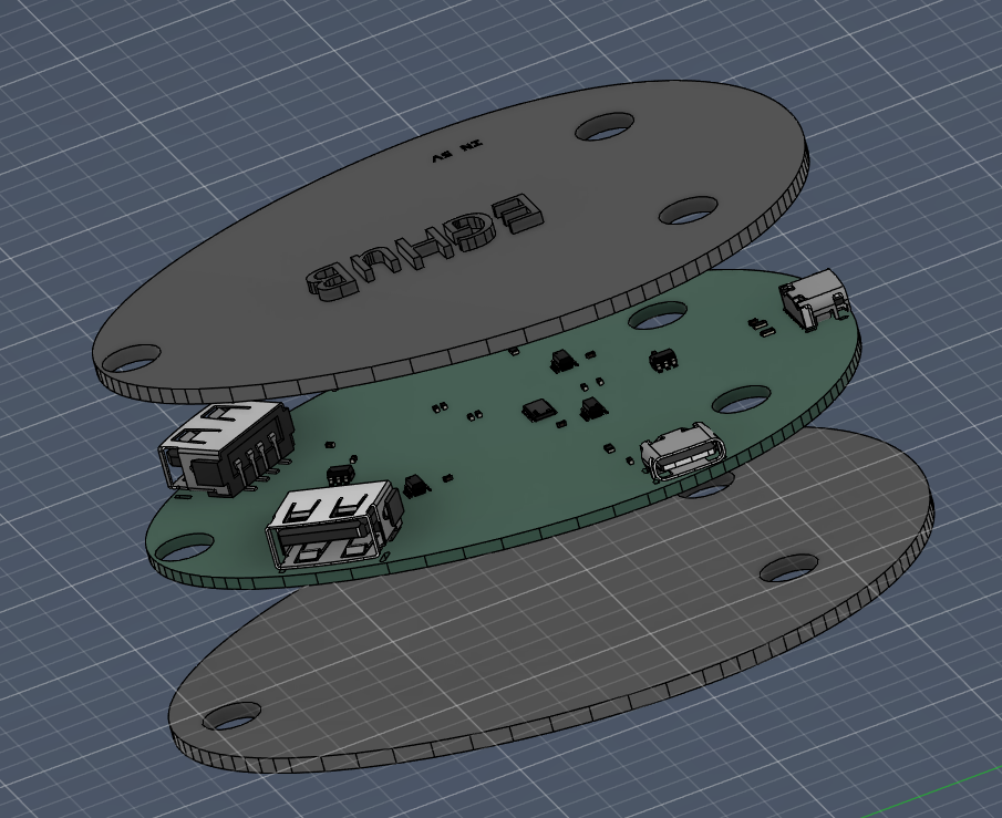
| Qty | Value | Footprint | References |
|---|---|---|---|
| 8 | 100nF | Capacitor_SMD:C_0805_2012Metric_Pad1.18x1.45mm_HandSolder | C7, C9, C11, C12, C13, C14, C15, C16 |
| 8 | 1uF | Capacitor_SMD:C_0805_2012Metric_Pad1.18x1.45mm_HandSolder | C1, C2, C3, C4, C5, C6, C8, C10 |
| 6 | 5.1K | Resistor_SMD:R_0805_2012Metric_Pad1.20x1.40mm_HandSolder | R1, R2, R3, R4, R5, R6 |
| 5 | USBLC6-2SC6 | Package_TO_SOT_SMD:SOT-23-6 | U2, U3, U4, U5, U6 |
| 3 | TYPE-C 16PIN 2MD | easyeda2kicad:USB-C-SMD_TYPE-C-6PIN-2MD-073 | USB2, USB6, USB7 |
| 2 | 10.0 QHHTZB6.3 | easyeda2kicad:USB-A-TH_10.0QHHTZB6.3 | USB5, USB8 |
| 1 | SL2.1S | easyeda2kicad:SSOP-16_L4.6-W2.6-P0.53-LS4.0-BL | U1 |
It measures 66.5 × 89.2 mm and has 2 copper layers, 1.6 mm thick.
33 parts, built around the SL2.1S and USBLC6-2SC6. The full list of its parts is on this page, with links to each part's symbol and footprint where PCBKit's library has them.
From the karhincheong/EgHub repository on GitHub, at the commit this page was made from: the board is kicad/USB_HUB.kicad_pcb and its schematic kicad/USB_HUB.kicad_sch. PCBKit opens the board in the browser, with nothing to install.
Its repository publishes it under the GPL-3.0 licence: you may reuse it on that licence's terms (keep the author's notice, and for a copyleft licence share your changes alike).
Gusus169/PRISM-The-usb-hub
A compact 4-port USB 2.0 hub PCB featuring ESD protection, PTC resettable fuses, and per-port LED indicators.


Lumethra/Auth75
This is a 75% keyboard with a fingerprint sensor. What? A fingerprint sensor in a keyboard? Yes, you've heard it right! This keyboard includes a working fingerprint sensor.

Lumethra/CADPad
SHHH, this is a gift, dont spoiler it, SHHHH. But what exactly is this?? Good question. Its a keyboard. Again. Wait, what does again mean, well its my second one. My Auth75 was my first one. Back to what this is.


DZ392/pcb-project
This is a small 4-port USB hub built into a butterfly-shaped PCB. Instead of using a cable like most USB hubs, it plugs directly into the side of a laptop.
