2 layers54 × 35 mm
Controller
kamilix2003/Phase-Shifter
Interface for RF phase shifter as part of phased antenna array
67 parts3MIT

 kamilix2003/Phase-Shifter3
Interface for RF phase shifter as part of phased antenna array
Feed network is an open-source printed circuit board by kamilix2003, from the kamilix2003/Phase-Shifter repository on GitHub, published under the MIT licence. It is a 2-layer board of 61.5 × 180 mm with 38 parts on 45 nets, routed with 365 tracks and 168 vias.
Its parts include 13 capacitors, 9 connectors, 4 resistors, 4 ICs and 1 crystal. It belongs with the radio and wireless and interfaces and adapters boards of this library.
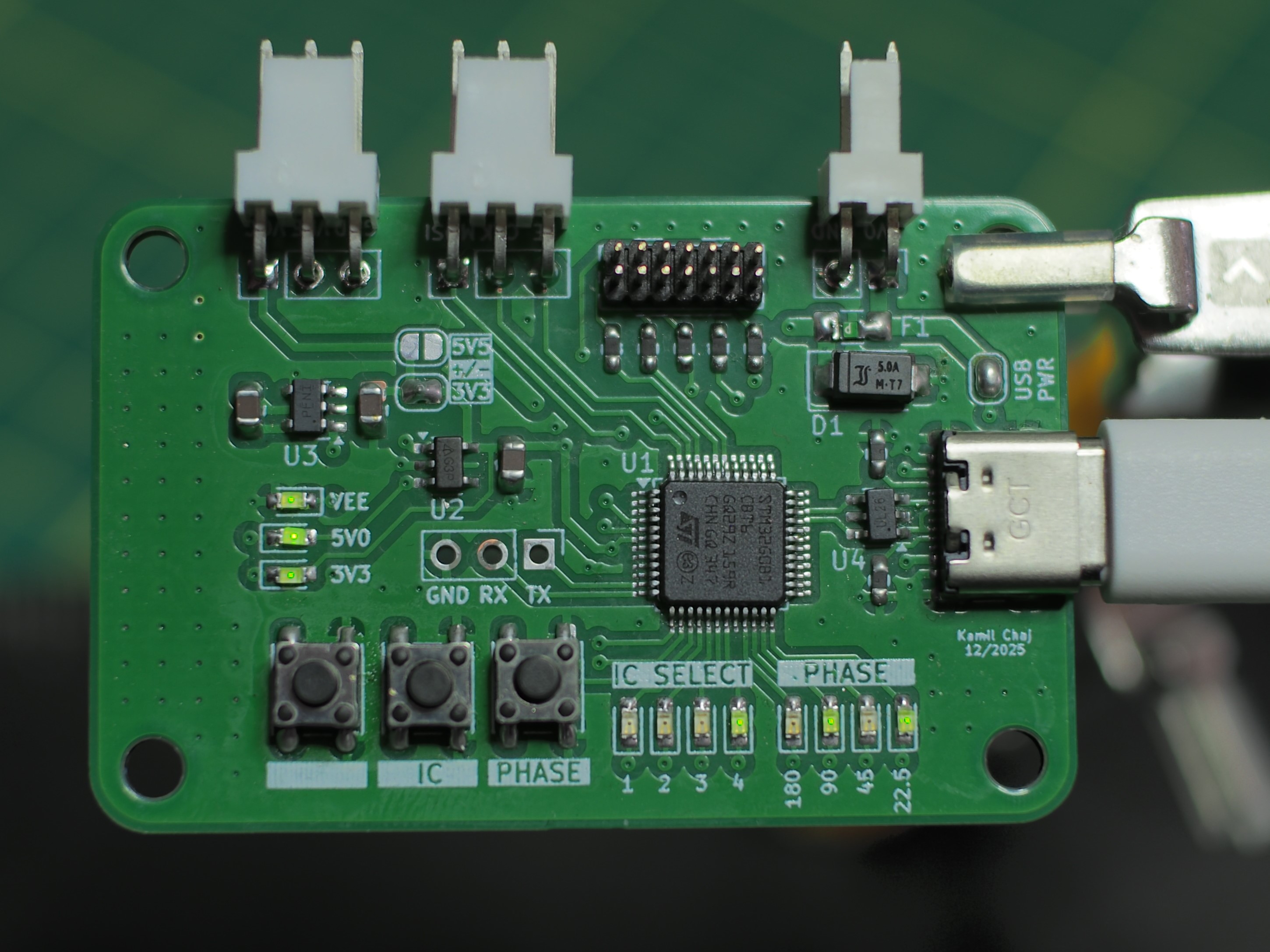
STM32G0B01 based board for controlling daisy-chained digital phase shifter via SPI-like serial interface. User can interface with the board either by buttons and LEDs on the board or via virtual serial port over USB, communication over serial port is realized using simple TLV protocol. The board is providing bipolar supply for the phase shifters.

Available commands:
| Type | Length [bytes] | Value | Description |
|---|---|---|---|
| 0x02 | 1 | command id | Ack |
| 0x10 | 4 | phase shifts (0 - 15) | Set phase |
| 0x11 | 0 | - | Transmit |
| 0x12 | 1 | latch state | Latch state |
After each message microcontroller should send ACK message with payload containing command id of original message
Example routine to set new phase delay:
0x12 0x01 0x00 - make sure that latch is set low in order to accept data via serial interface0x10 0x04 0x04 0x02 0x0f 0x08 - send phase shifts to the controller0x11 0x00 - transmit phase shifts via SPI to the phase shifters0x12 0x01 0x01 - set latch to update phase shift0x12 0x01 0x00 - reset latchThe board is equiped in 3 tactile buttons and two 4-led displays where each display shows according to the silkscreen description either currently selected phase shifter or phase shift set for the selected phase shifter. Buttons have following functions starting from the left most button:
| Qty | Value | Footprint | References |
|---|---|---|---|
| 8 | 100n | Capacitor_SMD:C_0603_1608Metric_Pad1.08x0.95mm_HandSolder | C1, C2, C3, C4, C5, C6, C7, C8 |
| 7 | MountingHole | MountingHole:MountingHole_3.2mm_M3 | H1, H2, H3, H4, H5, H6, H7 |
| 5 | 47p | Capacitor_SMD:C_0603_1608Metric_Pad1.08x0.95mm_HandSolder | C9, C10, C11, C12, C13 |
| 5 | ~ | Phase_shifter:Conn | J1, J2, J3, J4, J5 |
| 4 | 5.1k | Resistor_SMD:R_0603_1608Metric_Pad0.98x0.95mm_HandSolder | R1, R2, R3, R4 |
| 4 | Conn_02x04_Odd_Even | Connector_PinHeader_2.54mm:PinHeader_2x04_P2.54mm_Vertical | J6, J7, J8, J9 |
| 4 | ~ | Phase_shifter:QFN-24_EP_4x4_Pitch0.5mm | U1, U2, U3, U4 |
| 1 | ~ | Phase_shifter:4_way_divider | X1 |
kamilix2003/Phase-Shifter
Interface for RF phase shifter as part of phased antenna array

kamilix2003/Phase-Shifter
Interface for RF phase shifter as part of phased antenna array

kamilix2003/Phase-Shifter
Interface for RF phase shifter as part of phased antenna array

kamilix2003/Phase-Shifter
Interface for RF phase shifter as part of phased antenna array

kamilix2003/Phase-Shifter
Interface for RF phase shifter as part of phased antenna array

joeycastillo/The-Open-Book
For details on how to build, test and use Open Book, I've made documentation available here.


hackclub/OnBoard
💡 Join 1,000 teenagers and make your first PCB with a $100 grant!


Ardumower/ardumower
Develop an open source robotic lawn mower (HW+SW reference platform)

CRImier/MyKiCad
My KiCad boards. Can't be bothered uploading individually anymore, so here you go.


It measures 61.5 × 180 mm and has 2 copper layers, 1.6 mm thick.
38 parts. The full list of its parts is on this page, with links to each part's symbol and footprint where PCBKit's library has them.
From the kamilix2003/Phase-Shifter repository on GitHub, at the commit this page was made from: the board is KiCAD/Feed_network/Feed_network.kicad_pcb and its schematic KiCAD/Antenna_array/Antenna_array.kicad_sch. PCBKit opens the board in the browser, with nothing to install.
Its repository publishes it under the MIT licence: you may reuse it on that licence's terms (keep the author's notice, and for a copyleft licence share your changes alike).