4 layers45 × 16.5 mm
HadesGPSDongle
pms67/HadesFCS
Complete flight control system designed from scratch. Hardware designed with KiCad.
27 parts1kBSD-3-Clause

 kabbi/led-cube-factory
Vibe-coded scripts to generate PCBs with lots of leds
Square30-dense is an open-source printed circuit board by kabbi, from the kabbi/led-cube-factory repository on GitHub. It is a 4-layer board of 30 × 30 mm with 27 parts on 9 nets, routed with 83 tracks and 8 vias.
Its parts include 8 capacitors and 4 connectors.
Parametric generator for tileable LED PCB tiles (KiCad 10). One YAML file per board variant; everything else -- footprints, pinouts, design rules, the hand-drawn back side -- is shared.
Browse every board and shape in the docs → · What we tried and why: experiments →
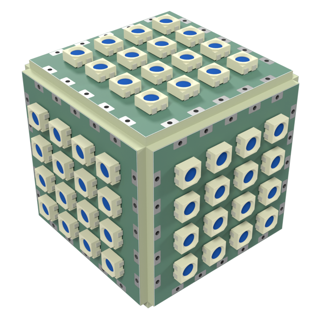
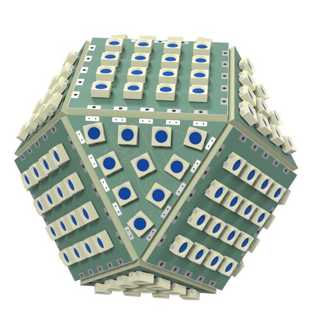
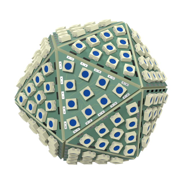
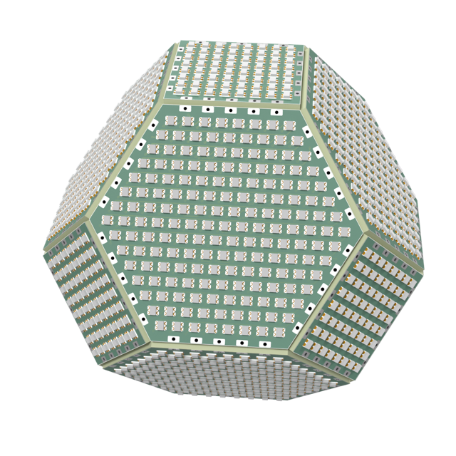
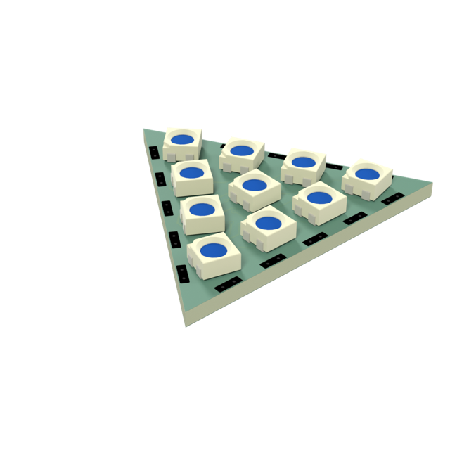
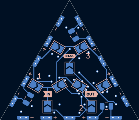
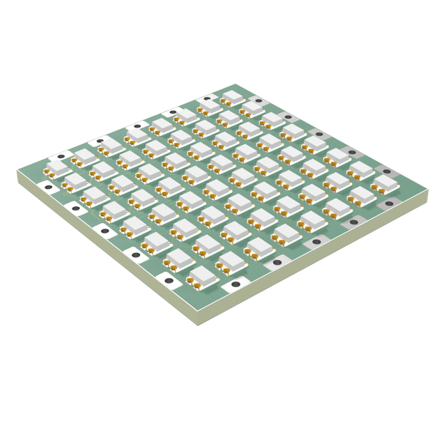
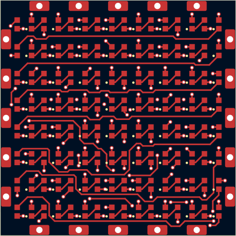
make setup                                 # once: venv on KiCad's Python + KiKit
make all                                   # build + DRC + render + fab every board, then tests
make all BOARDS=sq30-2020x64-p3.4-tpl      # just one
make panel PANELS=tri30-mix-4             # panels from panels/*.yaml (boards built first)
make release BOARDS=sq30-2020x64-p3.4-tpl  # freeze into releases/sq30-2020x64-p3.4-tpl-A/ before ordering
Tool paths default to the macOS app installs and can be overridden: make setup KICAD_PY=/path/to/kicad/python3 (a Python that can import pcbnew), kicad-cli and blender are taken from PATH first, and FREEROUTING_JAR / KICAD10_SYMBOL_DIR point at Freerouting and KiCad's symbol library.
boards/            one YAML per variant (the only thing you normally touch)
shapes/            one YAML per demo assembly (solid + boards)
lib/
  parts.yaml       part catalog: footprint, pin map, LCSC code per part
  defaults.yaml    defaults every board inherits (stackup, rules, router...)
  tbc.pretty/      shared footprints (vendored, so KiCad updates can't move them)
  tbc.3dshapes/    3D models not in KiCad's stock library
  tbc.kicad_dru    shared custom DRC rules
  templates/       hand-drawn "chassis" boards (outline, connectors, back side)
panels/            one YAML per panel (which boards where) + KiKit presets
tbcgen/            the generator
  geometry.py      outlines, ports, LED grids, chain order (pure Python)
  board.py         pcbnew: placement, routing order, planes
  router.py        small grid A* router (front data chain, power vias)
  outputs.py       project files, DRC, renders, fab, panel, release
  panel.py         panel layouts, tabs and mousebites (on KiKit)
  models.py        board GLBs, polyhedra assembled from them
  docs.py          docs/ pages from build/
tools/
  extract_template.py   pull a chassis template out of a hand-made board
  render_glb.py    GLB -> PNG with headless Blender
tests/             catalog/geometry checks + checks on built boards
build/<board>/     generated, git-ignored: KiCad project, drc.json, renders/,
fab/ (gerbers zip, BOM, CPL), pixelmap.json, 3d/template: square30 the board starts as a copy of
lib/templates/square30.kicad_pcb: outline, edge connectors J1..J4, caps,
the IN/OUT/PASS jumper hubs and all of their hand-drawn back routing. The
generator never adds or changes anything on B.Cu; it only checks the
template matches the board's shape (connector positions, net names).
Without a template, the chassis and back routing are generated (works
for any shape; see "Generated mode").leds:, all in one orientation
(rotation: auto), chained row by row (chain: raster). Pin roles come
from lib/parts.yaml, never from the footprint's pad order.kicad-cli pcb drc (zones refilled and saved -- the gerbers
are plotted from the saved fill), must be 0 errors and
0 unconnected; tests check the back is bit-for-bit the template.| template | from | for |
|---|---|---|
square30 | thecube/led_board_v5 | 30 mm square, sparse LEDs (5050) |
square30-dense | thecube/denser_v4 | 30 mm square, 3.4 mm grid; its vias sit in the LED gaps |
The back side's through vias (the inner-layer hops) come up on the front, so
a template has to suit the LED grid -- that's why there are two. To change
the back art, open the template in KiCad, edit, save, make all. To start
a new one, draw it by hand in a board and run
tools/extract_template.py SRC.kicad_pcb lib/templates/NAME.kicad_pcb.
Template contract: centre at (100, 100), connectors J1..Jn clockwise from
the top, nets P1..Pn, WS_IN, WS_OUT, PASS, +5V, GND, and WS_IN/WS_OUT
each ending in a via (the generator routes from there to the first/last LED).
Template parts keep their values and BOM flags (e.g. the 10 uF caps are
excluded from BOM/CPL, as in the original boards).
# boards/sq30-5050x9-p9-tpl.yaml
shape: square
edge: 30.0
leds: {part: ws2812b-5050, cols: 3, rows: 3, pitch: 9.0}
template: square30
The file name spells out the board and is checked against the config
(tbcgen/config.py: board_name), so a misnamed file fails to load and the
error says what to call it:
<shape><edge>-<package>x<leds>-p<pitch>[-<variation>...][--<note>]
tri30-3535x10-p6.2-shallow-rot
Variations, in this order: tpl hand-drawn back (template), shallow /
micro shallow or micro edge connector, rot / flow / r<deg> LED
rotation other than one-way auto, grp jumpers grouped by port, nopass
no PASS hub, pvia patterned power vias, fr Freerouting. Anything after
-- is a free note for experiments that the scheme doesn't cover.
New LED package: add the footprint to lib/tbc.pretty, an entry to
lib/parts.yaml with its pins map and kicad_symbol; the test suite
cross-checks the pin map against KiCad's stock symbol.
shape: tri | square | hex builds connectors on every edge, caps, three
jumper hubs (hubs:; one jumper per port, with the square30 KiBuzzard
labels tbc:label_in/out/pass in the middle) and auto-routes the back. It's
the way to prototype new shapes before drawing a template; expect to tune
hubs.jumper_radius (6 ports need ~4.3 mm) and leds.pitch.
Knobs the generated back offers, each worked out in an experiment:
connector: edge_connector_shallow (edge_conn_shallow:
pads 0.95 mm deep, two 0.3 mm holes each; same positions and pinout, so it
mates with the squares) for triangles; edge_connector_micro
(edge_conn_micro: 0.8 mm pads at 1.3 mm pitch, solid to the planes) for
the small tiles, which mate only with each other.radius, jumper_radius, angle (turns the layout: 180
often frees a boxed-in port), label_offset; on triangles keep
radius - jumper_radius >= 2.4, on hexagons jumper_radius: 4.3,
radius: 8. layout: grouped puts an IN/OUT pair by each port instead of
a cross per hub (spacing, inset, orient: along); roles drops hubs
(e.g. no PASS).jumper: jumper_small (1.45 x 0.8 mm) where the
1.3 mm ones don't fit; caps.ports puts caps on some ports only.rotation: edge turns each outer LED flat to its edge in 15 deg
steps (triangles; costs patterned vias). Hexagons take leds.rings (1, 7,
19, 37, ...).rules: {track_width: 0.127, clearance: 0.1, hole_copper_clearance: 0.2}, JLC's multilayer minimums.panels/<name>.yaml puts built boards on one panel (make panel, output in
build/panels/<name>/: the panel, panel.png, JLC gerbers, BOM and CPL with
per-board designators D1_3, and a DRC report):
preset: jlc-rails      # panels/jlc-rails.json: 5mm rails, tooling, fiducials, mousebite style
layout: tri            # grid | tri (rows alternating apex up/down, nested) | vcut
board: tri30-3535x10-p6.2-shallow-rot
rows: 2
cols: 5
space: 2.0             # mm between boards and to the rails
max_size: [100, 100]   # fail if the panel comes out bigger
# or, mixed: boards: [[a, b, c, d], ...] instead of board/rows/cols| panel | size | boards |
|---|---|---|
sq30-2020x64-p3.4-tpl-3x2 | 90 x 70 mm | 6; V-cut (3x3 fits 100 x 100) |
sq30-3535x16-p6.2-pvia-3x2 | 90 x 70 mm | 6; V-cut (3x3 fits 100 x 100) |
tri30-3535x10-p6.2-shallow-rot-2x5 | 99.2 x 68.0 mm | 10 (3 rows, 15, still fit 100 x 100) |
tri30-mix-4 | 81.9 x 40.0 mm | one of each triangle |
hex30-5050x37-p8-pvia-3x2 | 184.0 x 119.9 mm | 6 |
hex30-2020x169-p3.7-pvia-3x2 | 184.0 x 119.9 mm | 6 |
sq15-micro-mix-24 | 90 x 70 mm | 12 x 2x2 5050, 12 x 4x4 2020; V-cut (6 x 6 fit 100 x 100) |
sq8-5050x1-p5.5-micro-grp-nopass-pvia-11x6 | 88 x 58 mm | 66; V-cut (12 x 11 fit 100 x 100) |
Hexagons in a grid meet corner to corner side by side, so their tabs are on the flat top and bottom edges only.
The connector pads take the middle 22.5 mm of every edge, so tabs only fit in
the ~3.7 mm next to each corner (measured per board). Mousebites have to
cover the whole joint -- tab plus the fillets a 2 mm cutter leaves either side
(post.millradius), and at a junction of triangle corners everything the
cutter can't reach -- so the cut lines are read off the panel as milled, not
planned: any joint that would reach copper fails the build. Holes sit just
outside the board edge (offset: -0.25mm), clear of the inner planes, so
expect small nubs near the corners after breaking out. A mixed panel's DRC
uses the finest rules among its boards (each has passed its own DRC).
Square panels go on layout: vcut (preset jlc-vcut): boards edge to edge,
split by V-cuts alone, no tabs, so no nubs and no 2 mm gaps. Triangles and
hexagons stay on tabs: V-cuts are straight lines only. A V-cut runs across
the whole panel, so each column is one tile width and each row one tile
height (bands); . is scrap where bands of different sizes cross. Why, and
the trade-offs: V-cut panels vs tabs.
layout: vcut
legend: {A: sq15-5050x4-p7.5-micro-pvia, c: sq8-5050x1-p5.5-micro-grp-nopass-pvia}
boards:
  - A A . .
  - . . c c
The cuts go on every band boundary and against the rails, on Cmts.User
(KiKit's JLC export sends that layer as V-CUT). The edge pads sit 0.115mm
from the cut, against JLC's usual 0.4mm for copper by a V-cut, so the score
skims the pads' outer edge, and JLC may query the order. Where the mask
openings of facing pads merge across a cut (the dense template's do), panel
DRC waives the solder mask bridge: it pairs two boards' nets and sits on the
cut line. Waivers are listed as waived:<type> in the panel output.
router.engine: internal (default) is the in-house grid router.
router.engine: freerouting round-trips through Specctra DSN/SES with
Freerouting 2.x run headless (--gui.enabled=false, neckdown off; extra
settings via router.freerouting_settings). Template copper is locked and
nets are restricted to F.Cu (use_layer); the template's inner-layer hops
are swapped for via keep-outs (2.x refuses planes that carry traces) and
restored exactly after the SES import, along with the rest of the template.
Data-chain links it leaves open are finished by the in-house router.
It never beat the in-house router on these boards:
Freerouting vs the in-house router.
router.power_vias: nearest (default) gives each LED power pad a via at the
closest free spot. pattern (tbcgen/vias.py) reserves corridors for the
data chain (in-row links + a return band per row gap), then picks one
LED-relative VDD/GND via offset that fits the most LEDs against everything
already on the board (template back copper, pads, edge, holes) and repeats it
on every LED; misfits get the nearest spot outside the corridors. On the 2020
it chooses both vias under the LED body, between the pad columns.
Patterned vias line up in columns on the back, leaving channels for the port/hub routing; that's what lets dense boards route without a hand-drawn template (numbers). In2 hops are cheap but must not enclose plane areas.
make model                                   # build/<board>/3d/<board>.glb for every built board
make shapes                                  # build/shapes/<shape>.glb for every shapes/*.yaml
make shapes SHAPES=cube--sq30-2020x64-p3.4-tpl
A shape is a small file in shapes/, named like a board from what's in it
(<solid>--<square board>+<tri board>, checked on load); its header
comment becomes its description in the docs:
# shapes/cube--sq30-2020x64-p3.4-tpl.yaml
# The dense cube: six 8x8 2020 tiles on the hand-drawn dense back, 384 LEDs.
solid: cube
boards: {square: sq30-2020x64-p3.4-tpl}
Solids: tetrahedron, cube, octahedron, icosahedron, square-pyramid,
triangular-prism, cuboctahedron, hexagonal-prism, truncated-tetrahedron,
truncated-octahedron (tbcgen/models.py: SHAPES; any solid whose faces are
regular triangles, squares and hexagons can be added as a vertex list).
A shape names its boards <square>+<tri>+<hex>, only those the solid uses.
Each tile sits with its board bottom on the face and LEDs out, so neighbours
meet along their inner edges, as on a real build. A board's GLB is merged
per material and instanced on every face, so a solid's file is about the
size of one tile per board type. GLBs open in Blender or any glTF viewer
(Finder / Quick Look don't preview them).
With Blender installed (blender on PATH or /Applications/Blender.app),
both commands also write a PNG preview next to each GLB:
tools/render_glb.py runs headless (Cycles on CPU, transparent background,
three-quarter view fitted to the model), ~10 s per board and ~35 s per solid
at 1200 px. Render any GLB by hand with
blender -b --factory-startup -P tools/render_glb.py -- in.glb out.png 1200.
make docs writes docs/ from build/: an index, a page
per board (description from its YAML header comment, config, name breakdown,
DRC and routing numbers, top/bottom renders, the four copper layers, 3D
render, pixel map) and a page per shape (render, tiles and LED count, links
to its boards). Images are copied next to each page, so docs/ is
self-contained and meant to be committed. Full refresh:
make all model shapes docsparts.yaml, rules in
defaults.yaml, connector/back art in templates. Boards only say what
differs.tbc: via a project-relative fp-lib-table.build/ is ignored); what was ordered
is frozen in releases/ with its config, DRC report and fab files.build/<board>/<board>-failed.kicad_pcb for inspection.jlc_rotation per part to
correct); check the JLC assembly preview on the first order of a package.| Qty | Value | Footprint | References |
|---|---|---|---|
| 12 | SolderJumper_2_Open | tbc:SolderJumper-2_P1.3mm_Open_TrianglePad1.0x1.5mm | JP1, JP2, JP3, JP4, JP5, JP6, JP7, JP8, JP9, JP10, JP11, JP12 |
| 8 | 10uF | tbc:C_0805_2012Metric | C1, C2, C3, C4, C5, C6, C7, C8 |
| 4 | Conn_01x05_Socket | tbc:edge_conn | J1, J2, J3, J4 |
| 1 | G*** | kibuzzard-6A25C4AE | kibuzzard-6A25C4AE |
| 1 | G*** | kibuzzard-6A25C488 | kibuzzard-6A25C488 |
| 1 | G*** | kibuzzard-6A25C4BE | kibuzzard-6A25C4BE |
pms67/HadesFCS
Complete flight control system designed from scratch. Hardware designed with KiCad.


loxodes/vna
Under development open hardware microwave vector network analyzer


MitkoDyakov/Calipatron
I design my own digital caliper based on STM32F103C8T6 blue pill.


alexbegoon/meshimi
Meshimi unlocks powerful mesh networking for your Flipper Zero combining Meshtastic, LoRaWAN and other protocols like Matter and Thread to give you rock‑solid connectivity across miles, even off‑grid.
It measures 30 × 30 mm and has 4 copper layers, 1.6 mm thick.
27 parts. The full list of its parts is on this page, with links to each part's symbol and footprint where PCBKit's library has them.
From the kabbi/led-cube-factory repository on GitHub, at the commit this page was made from: the board is lib/templates/square30-dense.kicad_pcb. PCBKit opens the board in the browser, with nothing to install.
Its repository states no licence, so its author keeps all rights: ask kabbi before reusing the design.