2 layers192.4 × 50 mm
 jyancat/EC-Debug2
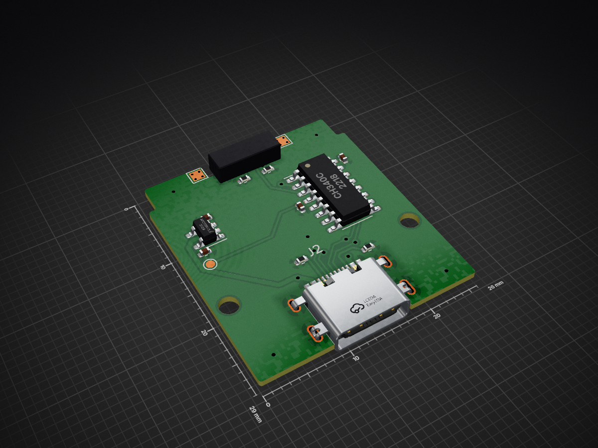
EC Debug is an open-source printed circuit board by jyancat, from the jyancat/EC-Debug repository on GitHub, published under the CERN-OHL-S-2.0 licence. It is a 2-layer board of 26 × 29 mm with 19 parts on 23 nets, routed with 93 tracks and 21 vias.
It is built around the CH340C, AP2112K-3.3 and GT-USB-7014F. Its parts include 4 capacitors, 4 resistors, 2 ICs and 2 connectors.


| Qty | Value | Footprint | References |
|---|---|---|---|
| 4 | 5.1k | Resistor_SMD:R_0402_1005Metric | R1, R2, R3, R4 |
| 4 | TestPoint | TestPoint:TestPoint_Pad_1.5x1.5mm | TP1, TP2, TP3, TP4 |
| 2 | 100nF | Capacitor_SMD:C_0402_1005Metric | C2, C4 |
| 2 | 1uF | Capacitor_SMD:C_0402_1005Metric | C1, C3 |
| 2 | MountingHole | MountingHole:MountingHole_2.2mm_M2 | H1, H2 |
| 1 | 3V3 | TestPoint:TestPoint_Pad_D1.0mm | TP5 |
| 1 | AP2112K-3.3 | Package_TO_SOT_SMD:SOT-23-5 | U1 |
| 1 | CH340C | Package_SO:SOIC-16_3.9x9.9mm_P1.27mm | U2 |
| 1 | GT-USB-7014F | EC Debug:GT-USB-7014F | J2 |
| 1 | USB_C_Plug_USB2.0 | EC Debug:105444 | P1 |
It measures 26 × 29 mm and has 2 copper layers, 0.8 mm thick.
19 parts, built around the CH340C, AP2112K-3.3 and GT-USB-7014F. The full list of its parts is on this page, with links to each part's symbol and footprint where PCBKit's library has them.
From the jyancat/EC-Debug repository on GitHub, at the commit this page was made from: the board is Hardware/EC Debug.kicad_pcb and its schematic Hardware/EC Debug.kicad_sch. PCBKit opens the board in the browser, with nothing to install.
Its repository publishes it under the CERN-OHL-S-2.0 licence: you may reuse it on that licence's terms (keep the author's notice, and for a copyleft licence share your changes alike).

jpconstantineau/NRF52-Board
This Repository is a collection of NRF5x boards.

jyancat/UART-Expansion-Card
Design files for the UART expansion card, please note this is a tested and working expansion card. Licensed under CERN-OHL-S-2.0. Uses the CH340C with switchable power and logic levels (5V and 3V3)


sparkfun/SparkFun_UM980_Triband_GNSS_RTK_Breakout
Documentation and hardware repository for the SparkFun Triband GNSS RTK Breakout, featuring the UM980 high precision GNSS/RTK module from Unicore Communications

wenzel-lab/syringe-pumps-and-controller
Design of 3d printable syringe pumps and dual controller.

upsidedownlabs/MSP430G2553-Feather
MSP430G2553 based Adafruit feather compatible board 🪶
