0bCLK
11 LED Binary Clock using an ATmega48A
- Size
- 72.5 × 40 mm
- Copper layers
- 2
- Thickness
- 1.6 mm
- Parts
- 18
- Nets
- 25
- Pads
- 66
- Tracks, vias
- 74, 6
- Pours
- 2
- Routed
- Yes
- KiCad
- KiCad 7 (file 20221018)
- Created
- 16 Nov 2024
- Updated
- 1 Jul 2025
Overview
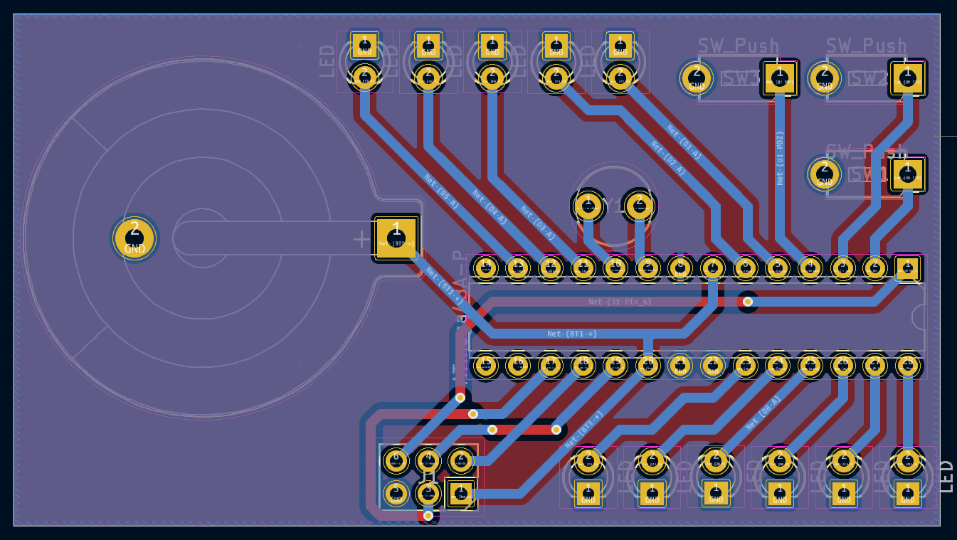
0bCLK is an open-source printed circuit board by Jvlse, from the Jvlse/0bCLK repository on GitHub. It is a 2-layer board of 72.5 × 40 mm with 18 parts on 25 nets, routed with 74 tracks and 6 vias.
It is built around the ATMEGA48A-PU. Its parts include 11 diodes, 3 switches, 1 IC, 1 connector and 1 crystal. It belongs with the AVR (ATmega, ATtiny) boards of this library.
Main components
1README
README.md0bCLK
11 LED Binary Clock using an ATmega48A, Datasheet
Code is here
FEATURES:
- Binary Time on 11 LED's with PWM brightnesscontrol
- Control over buttons
- Sleepmode with shown reduce of power
- Timebase using Timer and quartz crystal (accuracy can be messured at PB0)
- Flashing using ISP, for example using a USBasp and avrdude or an Arduino
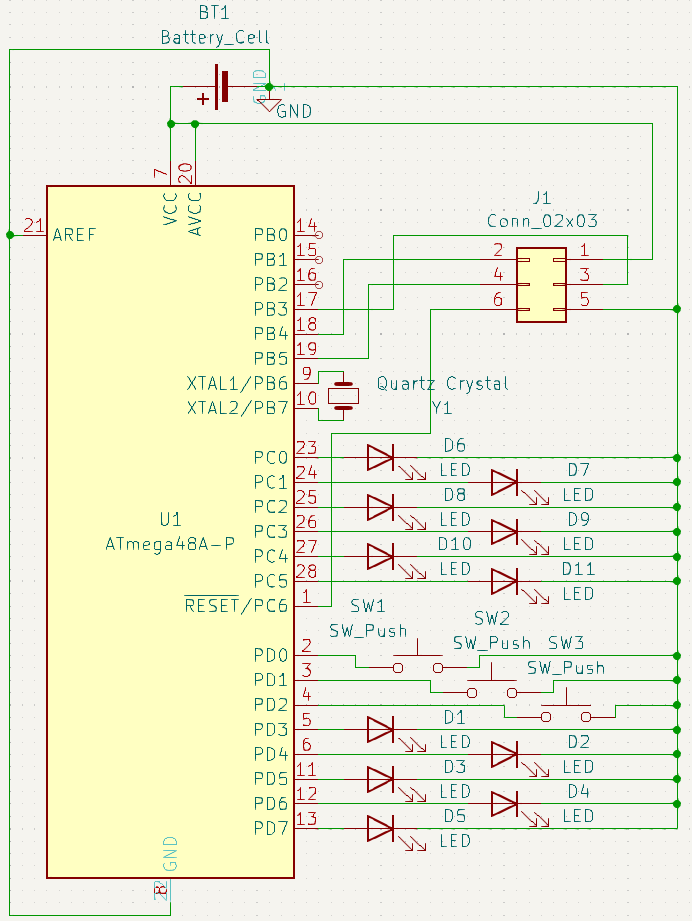
Schematic:

PCB:
- I used a mill for the 2-layer PCB
- All components are mounted on the top and soldered on the bottom
- I used CR2032 battery cells
- For orientation of the ISP:
- the square pad on the footprint is the VCC pin of the 6-pin ISP

Command for flashing using avrdude in Windows:
avrdude -c [programmer] -p m48A -Uflash:w:Path\To\CLK\Debug\CLK.hex:i
Example using USBasp, path is "C:\Atmel_Studio\7.0\CLK\Debug\CLK.hex":
avrdude -c usbasp -p m48A -Uflash:w:C:\Atmel_Studio\7.0\CLK\Debug\CLK.hex:i
Power saving:
- If CPU is doing nothing (waiting for Timer interrupt)
- goes to PWR_SAVE (basically completely off exept async Timer and interrupt)
- Disabling individual Timers, Two Wire Interface (TWI), Universal Synchronous Asynchronous Receiver Transmitter (USART0) and Analog Digital Converter (ADC)
- more optimizations: turning off Watchdog timer, brown out, lower CPU CLK, lower voltage, using sleepmodes
Fuse bits:
- SPIEN: LEAVE ON!
- else it won't be flashable using SPI/ISP anymore
- WDTON: OFF
- Watchdog timer not needed
- CKDIV8: OFF
- no system clock division needed
- BODLEVEL: Maybe
- if left off a brown out might lead to malfunction
Power usage:
- Default 6,5mA -> 35h runtime
- PWR_SAVE 1,2µA -> 191666h ~ 20 years runtime
CLK inaccuracy:
- Reasons:
- No Capacitors at quartz crystal, quartz temperature (25°C is optimal)
- Messuring:
- Output of Pulse Per Second (PPS) Signal at PB0 and meassuring using a counter
Timers:
- Timer 0: every ms for PWM
- Timer 2: every second for timebase
Buttons:
- PD0 -> down (PCINT16/RXD)
- PD1 -> up (PCINT17/TXD)
- PD2 -> mode (PCINT18/INT0)
Ports:
- Data Direction Register:
- DDR=0: Pin is input (button)
- DDR=1: Pin is output (LED)
- PORT-Register:
- if DDR=0
- 1: Pull-up resistor is active, for button
- 0: Pull-up not active
- if DDR=1
- 1: High voltage output
- 0: Low voltage output
- if DDR=0
Parts
18| Qty | Value | Footprint | References |
|---|---|---|---|
| 11 | LED | LED_THT:LED_D3.0mm | D1, D2, D3, D4, D5, D6, D7, D8, D9, D10, D11 |
| 3 | SW_Push | Button_Switch_THT:SW_PUSH_1P1T_6x3.5mm_H5.0_APEM_MJTP1250 | SW1, SW2, SW3 |
| 1 | ATmega48A-P | Package_DIP:DIP-28_W7.62mm | U1 |
| 1 | Battery_Cell | Battery:BatteryHolder_Keystone_106_1x20mm | BT1 |
| 1 | Conn_02x03 | Connector_PinSocket_2.54mm:PinSocket_2x03_P2.54mm_Vertical | J1 |
| 1 | Quartz Crystal | Inductor_THT:L_Radial_D6.0mm_P4.00mm | Y1 |
Questions
How big is the 0bCLK PCB?
It measures 72.5 × 40 mm and has 2 copper layers, 1.6 mm thick.
What parts does the 0bCLK use?
18 parts, built around the ATMEGA48A-PU. The full list of its parts is on this page, with links to each part's symbol and footprint where PCBKit's library has them.
Where can I download the 0bCLK KiCad files?
From the Jvlse/0bCLK repository on GitHub, at the commit this page was made from: the board is KiCad/KiCad.kicad_pcb and its schematic KiCad/KiCad.kicad_sch. PCBKit opens the board in the browser, with nothing to install.
Can I use the 0bCLK design in my own project?
Its repository states no licence, so its author keeps all rights: ask Jvlse before reusing the design.
Similar boards
- 2 layers

- 2 layers27.9 × 16.5 mm

- 2 layers42.7 × 13.7 mm

Stm32-mini12864
VoronDesign/Voron-Hardware
Cool Hardware designed by the Voron Design group
18 parts1.1kGPL-3.0 - 2 layers41.2 × 46.6 mm

- 2 layers44 × 51.3 mm

4272MAVcoder R4
hackclub/OnBoard
💡 Join 1,000 teenagers and make your first PCB with a $100 grant!
18 parts915 - 2 layers28.3 × 14.3 mm

Tap Photosensor PCB
VoronDesign/Voron-Tap
Tap is a nozzle-based z-probe for the V2 and Trident printer designs. The entire toolhead moves to trigger an optical switch. Tap offers many advantages:
18 parts716GPL-3.0 - 2 layers20.3 × 15.2 mm

L0 stepper driver
Luos-io/luos_engine
Open-source and real-time orchestrator for cyber-physical-systems, to easily design, test and deploy embedded applications and digital twins.
18 parts546MIT - 2 layers