2 layers103 × 30.5 mm

 JQIamo/Electronic_Sideband_Locking_Pluto4
Firmware to use ADALM Pluto for Electronic Sideband Locking systems
Esb pluto adapter is an open-source printed circuit board by JQIamo, from the JQIamo/Electronic_Sideband_Locking_Pluto repository on GitHub. It is a 2-layer board of 25.4 × 27.9 mm with 9 parts on 18 nets, routed with 22 tracks and 1 via.
Its parts include 5 resistors, 3 connectors and 1 capacitor. It belongs with the interfaces and adapters boards of this library.
This project consists of a custom firmware (hdl code) that can be loaded on an ADALM Pluto board to produce a carrier with a low-distortion sinusoidal phase modulation as well as a square wave reference with a resolution of 2ns.
To start working with the repository the following two commands need to be invoked:
git clone

git submodule update --init --recursiveThe bitfile can be generated following the instructions in the gateware folder's README file
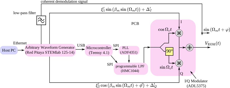
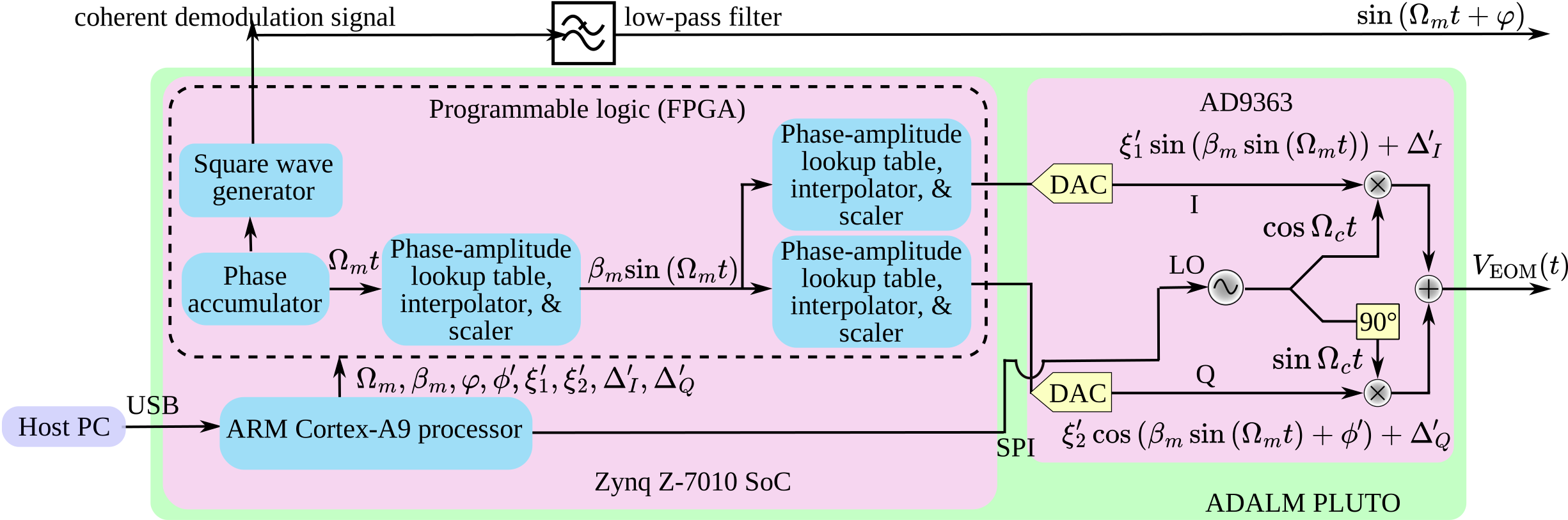
We present two architectures for generating the rf signal $V_{\textrm{EOM}}(t)$ and the phase-coherent demodulation signal $\sin \left(\Omega_m t+\varphi\right)$ for generating the electronic sideband (ESB) error signal. We refer to one of the architectures as the ADL5375-based design (see Figure 1) and the other variant as the ADALM-PLUTO-based design (see Figure 2). The baseband signals $I(t)$ and $Q(t)$ are digitally generated and reconstructed as analog signals by digital-to-analog converters (DACs) before being transmitted to quadrature modulators. The carrier wave is typically generated by filtering the square wave output of a Phase Locked Loop (PLL) integrated circuit. Both architectures are interfaced with a host PC. The host PC provides the values for all quadrature amplitude modulation (QAM) parameters: $\Omega_m, \Omega_c, \beta_m, \varphi, \phi', \xi_1', \xi_2', \Delta_I', \Delta_Q'$. The $\xi_1', \xi_2', \Delta_I', \Delta_Q', \phi'$ parameters help compensate for the intrinsic hardware I/Q impairments $\xi_1, \xi_2, \Delta_I, \Delta_Q, \phi$ by minimizing the RMS I/Q magnitude error. We elaborate on each design variant below.
The ADL5375-based design involves five modules, four of which are mounted on a custom printed circuit board (PCB). These modules are represented as pink boxes in Figure 1. The four modules on the custom PCB are a Teensy 4.1 microcontroller, an ADF4351 PLL chip, a HMC1044 programmable low-pass filter, and an ADL5375 I/Q modulator. The fifth module is a Red Pitaya STEMlab 125-14. These modules are connected to generate $V_{\textrm{EOM}}(t)$ as well as the phase-coherent demodulation signal.
The unfiltered carrier wave is generated by the ADF4351 phase-locked loop (PLL) chip, which has a frequency output in the range of $35$ MHz to $4400$ MHz. A $25$ MHz temperature compensated crystal oscillator (Murata Electronics XNCLH25M000THJA0P0) provides the reference frequency signal for the PLL chip. The PCB can be readily modified to take in an external reference clock. The lock time for the PLL chip is $\simeq1$ ms, which sets the minimum time it takes to update the carrier wave frequency. However, it can be decreased to $\simeq100~\mu\textrm{s}$ at the cost of increased phase noise. Furthermore, in our design, the PLL chip is controlled by the Teensy 4.1 microcontroller over a serial peripheral interface (SPI) bus. Specifically, a host PC command to update the frequency of the carrier wave is routed through the Red Pitaya STEMLab 125-14 to the Teensy 4.1., which then updates the values in the corresponding registers on the PLL chip via the serial peripheral interface (SPI).
The unfiltered carrier wave output of the PLL chip is a square wave. The square wave output must be filtered in order to generate a sinusoidal carrier wave. As the carrier wave frequency needs to be tunable over a broad frequency range, we need a low pass filter (LPF) with a tunable cut-off frequency. We use a programmable low-pass filter (HMC1044) with a tunable cutoff frequency in the range of 1 GHz to 3 GHz to remove the higher-order harmonics. Like the PLL chip, the programmable LPF is also controlled by Teensy 4.1 over SPI.
In addition to controlling Teensy 4.1 and interfacing with the host PC, STEMlab 125-14 also serves as the arbitrary waveform generator (AWG) that generates the baseband modulation signals $I(t)$, $Q(t)$, and the phase-coherent demodulation signal. A Python script running on the STEMlab 125-14 board is used to control the I/Q baseband signal synthesis. The STEMlab 125-14 board contains two fast $125$-mega-samples-per-second 14-bit DACs, and two $125$-mega-samples-per-second 14-bit analog-to-digital converters (ADCs). One of the digital input/output pins on the STEMlab 125-14 board is configured to output a square wave with a tunable phase at frequency $\Omega_{m}$. The square wave is filtered by a low-pass filter to yield the demodulation signal $\sin \left(\Omega_m t+\varphi\right)$. $\Omega_m$ is tunable as well. The baseband modulation and demodulation signals are phase-locked to each other as they share the same reference clock, which facilitates phase-coherent demodulation. The relative phase $\varphi$ between the signals is also programmable.
Lastly, the filtered sinusoidal carrier wave and the I/Q baseband signals are transmitted to the ADL5375 quadrature modulator. The quadrature modulator has a $400$ MHz to $6$ GHz output frequency range and a $-1$ dB baseband signal bandwidth of $\simeq400$ MHz. The quadrature modulator splits the carrier wave input internally to generate the in-phase and quadrature-phase carrier waves: $\cos(\Omega_{c}t),,\sin(\Omega_{c}t)$. The STEMlab 125-14 board provides the baseband signals that are transmitted to two of the four differential in-phase and quadrature-phase baseband inputs: QBBP, QBBN, IBBP, and IBBN. We externally DC bias the other two inputs. This arrangement converts the four differential baseband inputs to two single-ended baseband inputs: IBBP = QBBP = 0.5 V, IBBN = I(t) + 0.5 V, and QBBN = Q(t) +0.5 V. We use trimpots on the PCB to fine-tune the DC biasing of the IBBP, QBBP channels. This is done to null offsets between the differential inputs: IBBN - IBBP =I(t), QBBN - QBBP=Q(t). Furthermore, the offsets ($\Delta_I', \Delta_Q'$) in the baseband signal outputs can be programmed to perform fine offset nulling. Lastly, the PLL chip provides a differential power output with tunable power levels of $-4$ dB, $-1$ dB, $2$ dB, and $5$ dB referenced to one milliwatt, which we use to coarsely change the carrier level $\beta_c$. Fine control over $\beta_c$ is provided by controlling the amplitudes of the baseband signals $\xi_1'$ and $\xi_2'$ in STEMlab 125-14.
Here we present details on our modifications to the code base for the ADALM-PLUTO evaluation board to generate $V_{\textrm{EOM}}(t)$ and the phase-coherent demodulation signal $\sin \left(\Omega_m t+\varphi\right)$. The ADALM-PLUTO consists of two modules: an AD9363 rf agile transceiver Integrated Circuit from Analog Devices, and a Xilinx Zynq Z-7010 system-on-chip (SoC).
Two DAC channels and a broadband carrier wave oscillator, both of which are integrated into the AD9363, are used for QAM. The carrier wave frequency ranges from $325$ MHz to $3.8$ GHz with a tunable baseband channel bandwidth in the $200$ kHz to $20$ MHz range. The values of the parameters $\Omega_m,\Omega_c, \beta_m, \varphi, \xi_1', \xi_2', \Delta_I', \phi', \Delta_Q'$ are saved in FPGA registers that are mapped to the memory space of the ARM Cortex-A9 processor. The host PC can change their values by interacting with a local application on the processor that accesses these memory-mapped registers.
The baseband I/Q channel signals are generated by cascading two Direct Digital Frequency Synthesis (DDS) modules implemented in the programmable logic of the FPGA. A 32-bit phase accumulator and a 16-bit phase-amplitude lookup table, interpolator, and scaler convert the accumulated phase $\Omega_mt$ (that increments at the modulation frequency $\Omega_m$) to $\beta_m \sin \left(\Omega_m t\right)$. This $\beta_m \sin \left(\Omega_m t\right)$ serves as the accumulated phase for the last pair of phase-amplitude lookup tables, interpolators, and scalers: $\beta_m \sin \left(\Omega_m t\right)$ is mapped to $\xi_1'\sin(\beta_m \sin \left(\Omega_m t\right))+\Delta_I'$ for the I channel and $\xi_2'\cos(\beta_m \sin \left(\Omega_m t\right)+\phi')+\Delta_Q'$ for the Q channel. These digital baseband signals are then transmitted to the AD9363 transceiver, where they are reconstructed as analog I/Q waveforms. The AD9363 has a self-calibrating feature that we use to determine the values for $\Delta_I'$ and $\Delta_Q'$ to minimize carrier leakage errors. We manually tuned the phase offset ($\phi'$) and the baseband signal amplitudes ($\xi_1'$ and $\xi_2'$) to minimize the phase imbalance and gain imbalance errors.
In order to generate the phase-coherent demodulation signal $\sin \left(\Omega_m t+\varphi\right)$, we use one of the many $1.8$ V logic general purpose input/output (GPIO) ports on the ADALM-PLUTO board. The square wave output is referenced to the same phase accumulator used to generate the baseband signals. The square wave phase $\varphi$ is programmable. The square wave is low-pass filtered to generate the phase-coherent demodulation signal.
| Qty | Value | Footprint | References |
|---|---|---|---|
| 3 | R_US | Resistor_SMD:R_0603_1608Metric | R1, R2, R3 |
| 2 | Conn_Coaxial | Connector_Coaxial:SMA_Amphenol_901-144_Vertical | J2, J3 |
| 1 | 0 | Resistor_SMD:R_0603_1608Metric | R4 |
| 1 | C | Capacitor_SMD:C_0603_1608Metric | C1 |
| 1 | Conn_02x07_Odd_Even | Connector_PinHeader_2.54mm:PinHeader_2x07_P2.54mm_Horizontal | J1 |
| 1 | DNP | Resistor_SMD:R_0603_1608Metric | R5 |


FrameworkComputer/ExpansionCards
Reference designs and documentation to create Expansion Cards for the Framework Laptop

VoronDesign/Voron-Hardware
Cool Hardware designed by the Voron Design group

hackclub/OnBoard
💡 Join 1,000 teenagers and make your first PCB with a $100 grant!


adamws/kicad-kbplacer
KiCad plugin for automatic keyboard's key placement and routing
It measures 25.4 × 27.9 mm and has 2 copper layers, 1.6 mm thick.
9 parts. The full list of its parts is on this page, with links to each part's symbol and footprint where PCBKit's library has them.
From the JQIamo/Electronic_Sideband_Locking_Pluto repository on GitHub, at the commit this page was made from: the board is kicad/esb_pluto_adapter/esb_pluto_adapter.kicad_pcb and its schematic kicad/esb_pluto_adapter/esb_pluto_adapter.kicad_sch. PCBKit opens the board in the browser, with nothing to install.
Its repository states no licence, so its author keeps all rights: ask JQIamo before reusing the design.