2 layers116.8 × 30 mm
Type d
google/mozc-devices
Circuit diagrams and firmware source code for Gboard DIY keyboards
14 parts3kApache-2.0
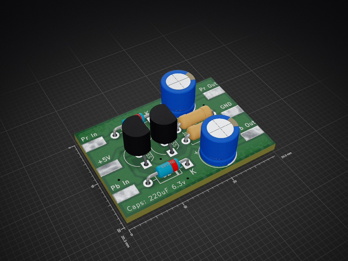
 joshman196/SNES-Component-Video-Mod-PCB
PCB that carries Pb and Pr video lines with their respective components.
Snesypbpr enhanced is an open-source printed circuit board by joshman196, from the joshman196/SNES-Component-Video-Mod-PCB repository on GitHub. It is a 2-layer board of 29.5 × 20.3 mm with 14 parts on 10 nets, routed with 33 tracks and 6 vias.
Its parts include 6 connectors, 2 capacitors, 2 resistors, 2 diodes and 2 transistors.
A PCB that carries Pb and Pr video lines with their respective components. The Y line is not on the PCB as we will just wire it directly from the multi-out port instead. This mod does not work on stock SNES Jr. or "1-Chip" consoles. Compatible stock consoles must contain an S-ENC chip. Sometimes the S-ENC chip is alternatively labelled as "BA6594AF" or may be a revision labelled as "S-ENC A" or "S-ENC B."
For RCA jacks, you only really need 3 just to do the mod since those will carry the video output and you can use the multi-out port for the audio, but you can choose to get 5 RCA jacks instead so you can also do Left and Right Audio alongside the YPbPr jacks if you prefer. This guide does not cover the installation of audio RCA jacks.
For the TRRS jack method, it's generally considered best to desolder and remove the RF modulator from the console and put the TRRS jack in its place. If you don't want to remove the RF modulator, you will have to come up with a spot to put the TRRS jack, like drilling a hole into the shell for it. Also, you can figure out which pin on the back of the jack corresponds to which YPbPr female connector by checking continuity with a multimeter with the adapter plugged into the TRRS jack. Touch one lead of the multimeter to a pin on the back of the jack and the other lead to the inside of one of the connectors to figure out which one is which. One pin on the back of the TRRS jack may be longer than the others. This one should be the Ground pin.
| Qty | Value | Footprint | References |
|---|---|---|---|
| 2 | 1N4148 | Diode_THT:D_DO-35_SOD27_P7.62mm_Horizontal | D1, D2 |
| 2 | 220uF 6.3V | Capacitor_THT:CP_Radial_D6.3mm_P2.50mm | C1, C2 |
| 2 | 75R | Resistor_THT:R_Axial_DIN0207_L6.3mm_D2.5mm_P7.62mm_Horizontal | R1, R2 |
| 2 | S8050/SS8050 | Package_TO_SOT_THT:TO-92_Inline_Wide | Q1, Q2 |
| 1 | +5V | Custom:SolderWirePad_1x01_SMD_2x4mm | J3 |
| 1 | GND | Custom:SolderWirePad_1x01_SMD_2x4mm | J4 |
| 1 | Pb In | Custom:SolderWirePad_1x01_SMD_2x4mm | J2 |
| 1 | Pb Out | Custom:SolderWirePad_1x01_SMD_2x4mm | J6 |
| 1 | Pr In | Custom:SolderWirePad_1x01_SMD_2x4mm | J1 |
| 1 | Pr Out | Custom:SolderWirePad_1x01_SMD_2x4mm | J5 |
google/mozc-devices
Circuit diagrams and firmware source code for Gboard DIY keyboards


hackclub/OnBoard
💡 Join 1,000 teenagers and make your first PCB with a $100 grant!


Twotoz/C5VRX
Ultra-minimal, zero-CPU 5.8 GHz analog FPV video receiver using ESP32-C5 Wi-Fi 6 PHY MODEM_DIAG, BitScrambler WBFM demodulation & resistor DAC CVBS


It measures 29.5 × 20.3 mm and has 2 copper layers, 1.6 mm thick.
14 parts. The full list of its parts is on this page, with links to each part's symbol and footprint where PCBKit's library has them.
From the joshman196/SNES-Component-Video-Mod-PCB repository on GitHub, at the commit this page was made from: the board is Standard/snesypbpr-enhanced.kicad_pcb and its schematic Standard/snesypbpr-enhanced.kicad_sch. PCBKit opens the board in the browser, with nothing to install.
Its repository states no licence, so its author keeps all rights: ask joshman196 before reusing the design.