2 layers40 × 34 mm
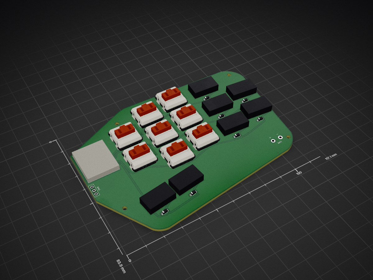
 jonnyirwin/eidolon
A small column-staggered wireless split keyboard. 30 keys (5×3 + 2 thumb per half), Kailh Choc v1 switches, Seeed XIAO nRF52840 BLE, Totem-style clamshell case. Both halves are independent wireless units — no TRRS cable.
Eidolon right is an open-source printed circuit board by jonnyirwin, from the jonnyirwin/eidolon repository on GitHub, published under the MIT licence. It is a 2-layer board of 117.1 × 83.9 mm with 37 parts on 32 nets, routed with 179 tracks and 20 vias.
Its parts include 16 switches and 15 diodes. It belongs with the keyboards and input boards of this library.
⚠️ Work in progress — do not build this yet. The PCB, case, and firmware have not been validated against a physical build. Things will change, things may be wrong. Watch the commits if you want to follow along, but don't order boards from these files yet.
eidolon /aɪˈdoʊlɒn/ noun An idealized image; a phantom or spectre of a person or thing. — from Greek εἴδωλον (image, idol, phantom)
A small column-staggered wireless split keyboard. 30 keys (5×3 + 2 thumb per half), Kailh Choc v1 switches, Seeed XIAO nRF52840 BLE, Totem-style clamshell case. Both halves are independent wireless units — no TRRS cable.
| Keyboard | Role in this project |
|---|---|
| Phantom by davidphilipbarr | PCB layout source — key positions reverse-engineered from lephantom.kicad_pcb; board outline traced from the original Edge.Cuts. Eidolon matches the original key centres to < 0.15 mm. |
| TOTEM by GEIGEIGEIST | Case design reference — switch hole dimensions, keycap recess depth, clamshell geometry, and hot-swap socket pocket profiles from the Totem STEP file; the XIAO BLE SMD footprint (pcb/footprints/xiao_ble.js) is adapted from Totem's xiao-ble-smd-cutout. |
| Rufous by jcmkk3 | Diode placement — diodes sit in each Choc south LED cutout following the Rufous approach. (pcb/footprints/xiao_pogo.js, a pogo-pin XIAO mount adapted from Rufous, is kept as an unused alternative to the SMD footprint.) |
| Left half | Right half |
|---|---|
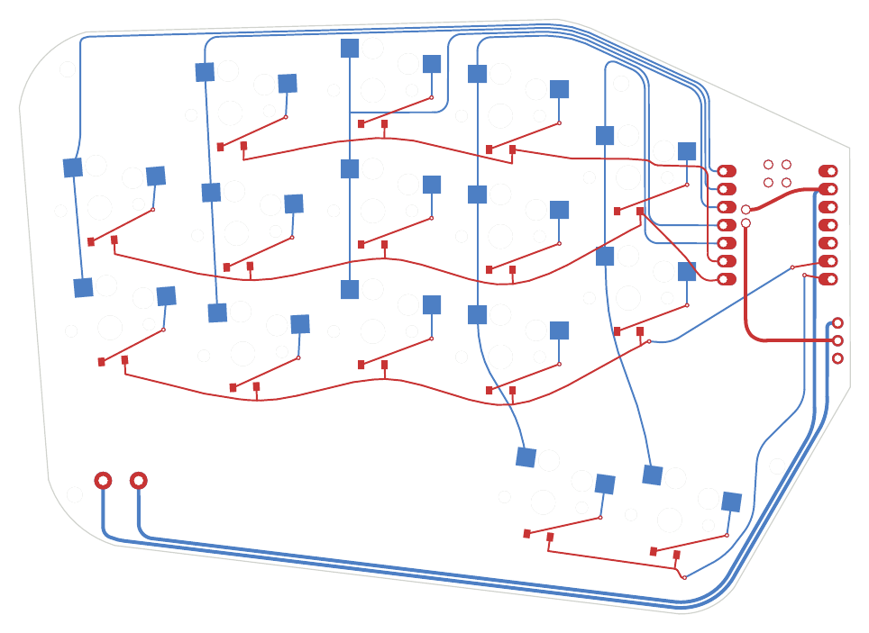 | 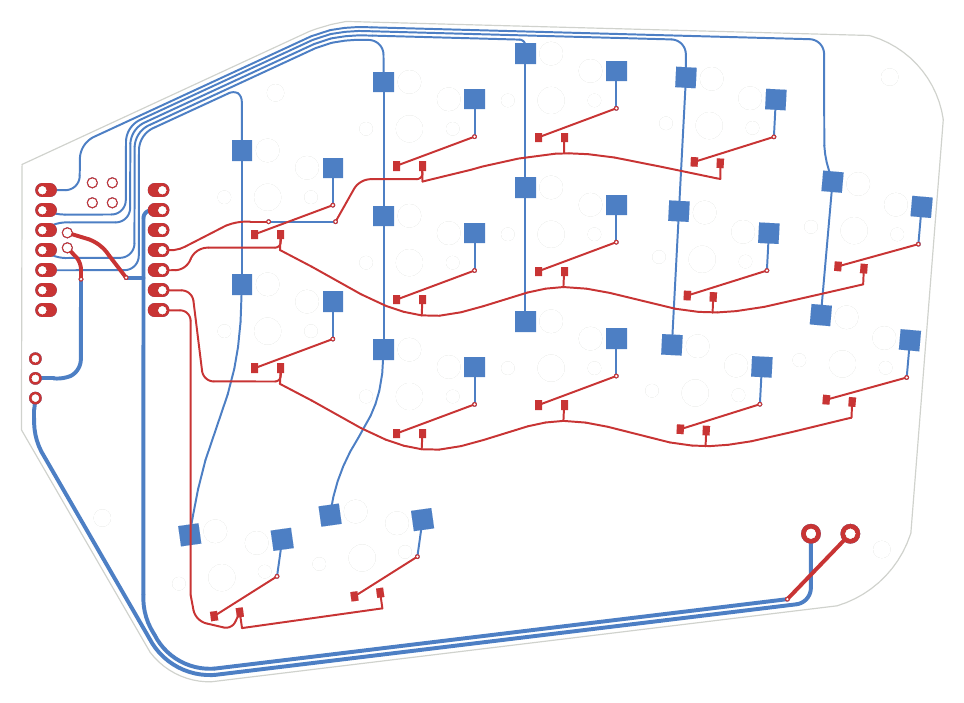 |
| Top — left | Top — right |
|---|---|
 | 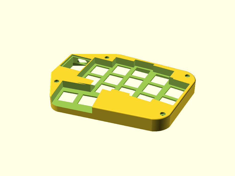 |
| Bottom — left | Bottom — right |
|---|---|
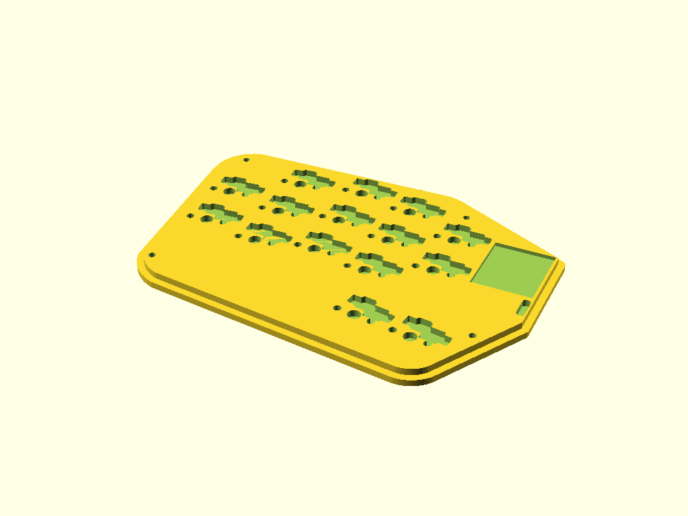 | 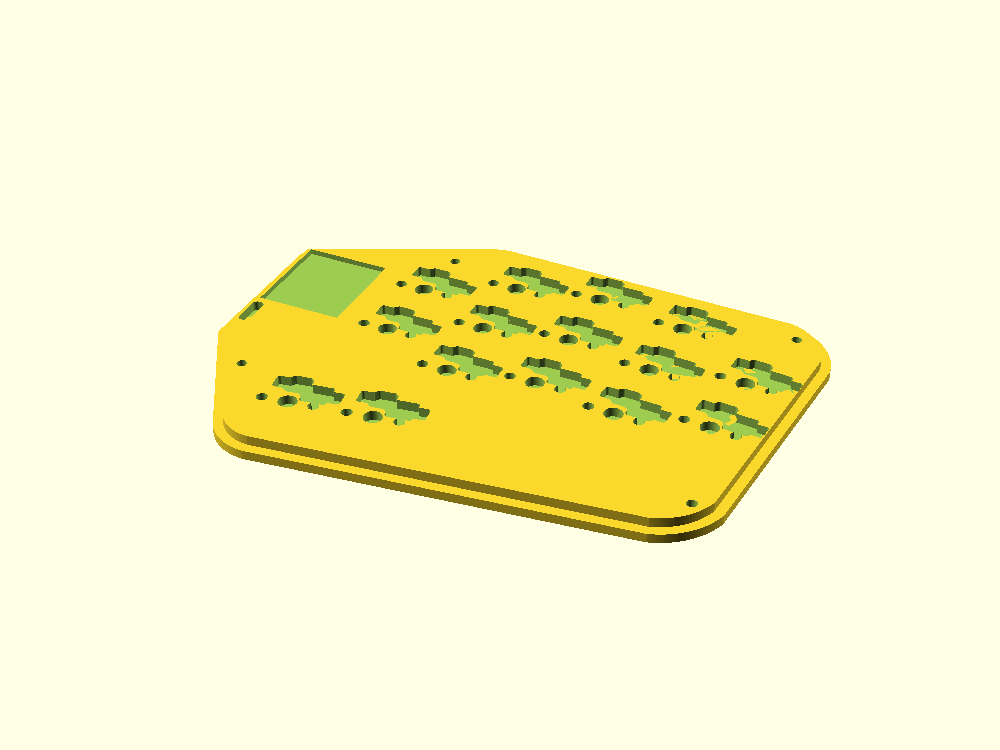 |
pcb/              Ergogen source + routed KiCad files + gerbers
  eidolon.yaml      Ergogen config (geometry + nets)
  footprints/       custom Ergogen footprints
  build.js          local build wrapper (injects footprints)
  eidolon_left.kicad_pcb   routed left half
  eidolon_right.kicad_pcb  routed right half
  eidolon_left_gerbers.zip
  eidolon_right_gerbers.zip

case/             OpenSCAD case design
  eidolon_case.scad        top shell (both halves via -D right=true)
  eidolon_case_bottom.scad bottom shell
stl/ pre-generated STL filesCustom footprints live in pcb/footprints/, so use the wrapper rather than the ergogen CLI directly:
cd pcb
npm install       # once
node build.js     # -> pcb/output/
Outputs land in pcb/output/:
outlines/board_left.svg|dxf, board_right.svg|dxf — board perimeterspcbs/eidolon_left.kicad_pcb, eidolon_right.kicad_pcb — both halves, footprints + nets placed (no routes)On ergogen.xyz, paste each file in pcb/footprints/ into the web app's Footprints section under its filename (e.g. reset_button); eidolon.yaml then works as-is.
 pinky  ring  middle index inner
   ·    top    top   top   ·       (pinky has no top row; inner has no bottom)
 home  home   home  home  upper
 bot   bot    bot   bot   lower
                  thumbL thumbR    (-8°)
Pinky splayed 5°, ring splayed 3°; other columns straight. Choc spacing: 18 mm columns, 17 mm rows.
Each half is a fully independent wireless unit (own XIAO + battery, no TRRS), so the two halves carry independent pin maps. The columns are identical; the rows are assigned per half to keep each MCU's fan-out clean.
| Matrix | Net | XIAO pin (left) | XIAO pin (right) |
|---|---|---|---|
| pinky col | C0 | D0 | D0 |
| ring col | C1 | D1 | D1 |
| middle col | C2 | D2 | D2 |
| index col | C3 | D3 | D3 |
| inner col | C4 | D4 | D4 |
| top row | R0 | D5 | D10 |
| home row | R1 | D6 | D9 |
| bottom row | R2 | D8 | D8 |
| thumb row | R3 | D7 | D7 |
On the right half all four rows sit on the matrix-facing D7–D10 edge (D5/D6 spare), so only the five columns cross the MCU — the physical minimum. The two halves therefore need different MATRIX_ROW_PINS in firmware.
Power: battery + → RAW_BATT → slide switch → BATT → XIAO B+; battery − → GND.
Verify before fab: the XIAO pad→pin mapping lives in
pcb/footprints/xiao_ble.js(surface-mount, mounted face-up over the PCB). It was corrected and checked against the XIAO datasheet and the TOTEMxiao-ble-smd-cutoutfootprint — re-confirm before ordering.
The original Phantom is a single reversible PCB flipped for both hands. Eidolon generates a true left and right board. Because each half is an independent wireless unit with its own firmware, the halves do not share a pin map — the right half's MATRIX_ROW_PINS differ from the left's (see the per-half table above).
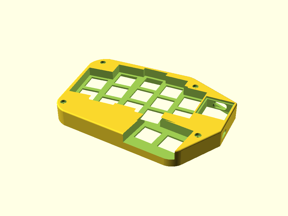
case/eidolon_case.scad is the top shell for both halves. The right half is the left mirrored (-D right=true).
openscad -o case/stl/eidolon_case_top_left.stl  case/eidolon_case.scad
openscad -D right=true -o case/stl/eidolon_case_top_right.stl  case/eidolon_case.scad
openscad -o case/stl/eidolon_case_bottom_left.stl  case/eidolon_case_bottom.scad
openscad -D right=true -o case/stl/eidolon_case_bottom_right.stl  case/eidolon_case_bottom.scad
Pre-generated STLs are in case/stl/.
Top shell features: keycap recess field, stepped 13.8 mm Choc plate holes, XIAO pocket with acrylic window rebate + USB-C cutout, battery pocket, power-switch wall slot, M2 bolt pockets.
case/eidolon_case_bottom.scad nests inside the top from below. Geometry:
floor_t = 2.0 mm) matching the top case outer footprintsocket_clr = 0.6 mm| Part | Spec | Count |
|---|---|---|
| Socket cap bolt | M2 × 12 mm | 4 per half |
| Hex nut | M2 (4.0 mm AF) | 4 per half |
Cut a piece of 1.5 mm clear acrylic to drop into the XIAO rebate:
| Dimension | Size |
|---|---|
| Width | 20.3 mm |
| Length | 22.8 mm |
| Thickness | 1.5 mm |
Angle the acrylic, slip the +y edge under the square lip (lip A), press the −y edge down past the chamfered lip (lip B). Remove the bottom shell to access the MCU.
ZMK firmware for the Eidolon is available at jonnyirwin/zmk-keyboard-eidolon.
Edge.Cuts polygon with 1.5 mm corner fillets.| Qty | Value | Footprint | References |
|---|---|---|---|
| 15 | diode_sod123 | D1, D2, D3, D4, D5, D6, D7, D8, D9, D10, D11, D12, D13, D14, D15 | |
| 15 | PG1350 | S1, S2, S3, S4, S5, S6, S7, S8, S9, S10, S11, S12, S13, S14, S15 | |
| 4 | mounting_hole_m2 | MH1, MH2, MH3, MH4 | |
| 1 | xiao_ble | MCU1 | |
| 1 | battery_pads | BT1 | |
| 1 | power_switch_spdt | SW1 |
It measures 117.1 × 83.9 mm and has 2 copper layers, 1.6 mm thick.
37 parts. The full list of its parts is on this page, with links to each part's symbol and footprint where PCBKit's library has them.
From the jonnyirwin/eidolon repository on GitHub, at the commit this page was made from: the board is pcb/eidolon_right.kicad_pcb. PCBKit opens the board in the browser, with nothing to install.
Its repository publishes it under the MIT licence: you may reuse it on that licence's terms (keep the author's notice, and for a copyleft licence share your changes alike).

hoglet67/RGBtoHDMI
Bare-metal Raspberry Pi project that provides pixel-perfect sampling of Retro Computer RGB/YUV video and conversion to HDMI

hackclub/OnBoard
💡 Join 1,000 teenagers and make your first PCB with a $100 grant!

FreeYourStream/freedeck-hardware
all the stuff you need to build your own FreeDeck

stuartpittaway/diyBMS
Do it yourself battery management system for Lithium ion battery packs/cells

Pwnsat/FlatSat
Flatsat v1.0 is a hardware based platform for aerospace cybersecurity research


vsfteam/vsf
Versaloon Software Framework -- a tiny preemptive-capable event-driven incremental software framework for embedded systems