2 layers368.3 × 215.9 mm

 jimbro1000/DragonDiscController1
Recreation of DragonDos disc controller cartridge
D32 disk controller is an open-source printed circuit board by jimbro1000, from the jimbro1000/DragonDiscController repository on GitHub, published under the MIT licence. It is a 2-layer board of 107.5 × 80.3 mm with 29 parts on 106 nets, routed with 1,011 tracks and 279 vias.
It is built around the 74HCT00D, 74HCT04D and 74HCT139D, with the 74HCT174D and 74HCT74D among its other parts. Its parts include 9 ICs, 6 resistors, 4 capacitors, 4 connectors and 1 diode.


This project contains the design and build
documents for a recreation of the DragonDos
disc controller
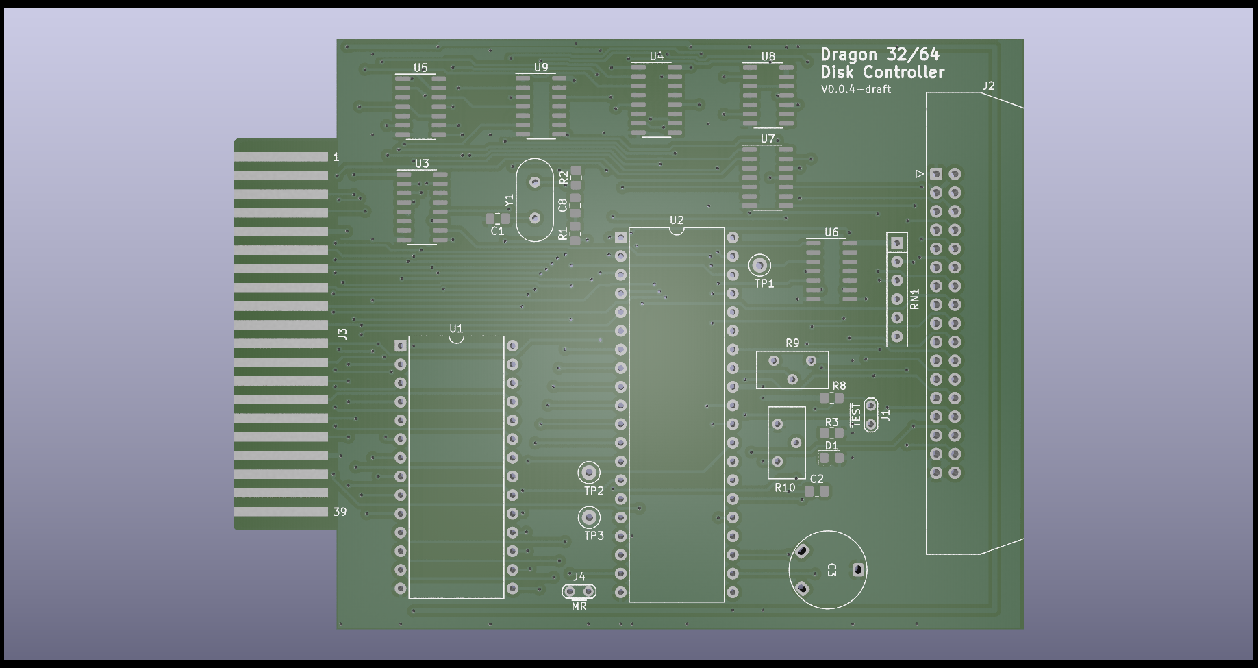
The schematics use a WDC WD2797 disc controller IC as the core of the board, this is consistent with the original DragonData design. Other 2797 ICs from different manufacturers should still work
Other than the rom and controller the discrete logic chips are surface mount to help with the availability of components. In all cases the surface mount parts are of the largest versions available to try and make the assembly of the board feasible for hand soldering
In the current state the board is untested
The PCB layout is (very) generous on dimensions and needs work to shrink it down. Iterating on this won't change the functionality and should significantly reduce the size of the board, and hence the cost of fabrication
Until the board progresses to a point where it can be tested the assembly instructions and the proven bill of materials are left unpublished
Adjust the RPW timing - measure the pulse width of the TG43 signal from pin 29 on U2. Use R10 to fix the pulse at 600ns
Adjust the WPW timing - measure the pulse width of the signal from pin 3 of U6, pin 31 of U2, or pin 22 of the IDC connector (the IDC pin is inverted). Use R9 to fix the pulse at 300ns
Adjust VC0 timing - measure the frequency of the DIRC signal from pin 1 of U6, pin 16 of U2, or pin 18 of the IDC connector (the IDC pin is inverted). Use C3 to set the signal at 250KHz
The official documentation identifies a more complex and thorough adjustment procedure. Where !TEST is referenced you can use the test point on the board at J1. Pin 1 is connected to !TEST on U2 (pin 22)
| Qty | Value | Footprint | References |
|---|---|---|---|
| 4 | 1K | Resistor_SMD:R_0805_2012Metric_Pad1.20x1.40mm_HandSolder | R1, R2, R3, R8 |
| 2 | 10K | Potentiometer_THT:Potentiometer_Bourns_3296Y_Vertical | R9, R10 |
| 1 | 10nF | Capacitor_SMD:C_0805_2012Metric_Pad1.18x1.45mm_HandSolder | C8 |
| 1 | 1N4148 | Diode_SMD:D_0805_2012Metric_Pad1.15x1.40mm_HandSolder | D1 |
| 1 | 220R | Resistor_THT:R_Array_SIP6 | RN1 |
| 1 | 220nF | Capacitor_SMD:C_0805_2012Metric_Pad1.18x1.45mm_HandSolder | C2 |
| 1 | 22pF | Capacitor_SMD:C_0805_2012Metric_Pad1.18x1.45mm_HandSolder | C1 |
| 1 | 27C64 | Package_DIP:DIP-28_W15.24mm | U1 |
| 1 | 4MHz | Crystal:Crystal_HC18-U_Vertical | Y1 |
| 1 | 5.5-65pf | d32_cart:Trimmer-10mm | C3 |
| 1 | 74HCT00 | Package_SO:SOIC-14_3.9x8.7mm_P1.27mm | U5 |
| 1 | 74HCT04 | Package_SO:SOIC-14_3.9x8.7mm_P1.27mm | U9 |
| 1 | 74HCT139 | Package_SO:SOIC-16_3.9x9.9mm_P1.27mm | U4 |
| 1 | 74HCT174 | Package_SO:SOIC-16_3.9x9.9mm_P1.27mm | U3 |
| 1 | 74HCT74 | Package_SO:SOIC-14_3.9x8.7mm_P1.27mm | U8 |
| 1 | 74LS06 | Package_SO:SOIC-14_3.9x8.7mm_P1.27mm | U6 |
| 1 | 74LS07 | Package_SO:SOIC-14_3.9x8.7mm_P1.27mm | U7 |
| 1 | EDGE | d32_cart:D32_Edge | J3 |
| 1 | IDC_Floppy | Connector_IDC:IDC-Header_2x17_P2.54mm_Latch_Horizontal | J2 |
| 1 | TestPoint_Probe | TestPoint:TestPoint_Loop_D2.50mm_Drill1.0mm | TP3 |
| 1 | TestPoint_TG43 | TestPoint:TestPoint_Loop_D2.50mm_Drill1.0mm | TP2 |
| 1 | TestPoint_WD | TestPoint:TestPoint_Loop_D2.50mm_Drill1.0mm | TP1 |
| 1 | WD2797 | Package_DIP:DIP-40_W15.24mm | U2 |
| 1 | ~{MR} | TestPoint:TestPoint_2Pads_Pitch2.54mm_Drill0.8mm | J4 |
| 1 | ~{TEST} | TestPoint:TestPoint_2Pads_Pitch2.54mm_Drill0.8mm | J1 |


leomil72/LM80C
A Z80-based homebrew computer withTMS9918, AY-3-8910, Z80 CTC, Z80 PIO, and Z80 SIO

AlexColello/discrete-nes
A discrete logic implementation of the Nintendo Entertainment System where EVERY single gate output and EVERY memory bit is visible via LED. Watch a complete NES flip every bit in real-time.

spaghetti-computer/lasagna
Status: schematic ERC 0 violations. PCB 100x100 mm, 2 layers, parts placed, NOT ROUTED (499 unconnected items). Freerouting 2.1.0 left about 271 nets unrouted after 4 passes. Do not order from fab/ yet.


It measures 107.5 × 80.3 mm and has 2 copper layers, 1.6 mm thick.
29 parts, built around the 74HCT00D, 74HCT04D, 74HCT139D and 74HCT174D. The full list of its parts is on this page, with links to each part's symbol and footprint where PCBKit's library has them.
From the jimbro1000/DragonDiscController repository on GitHub, at the commit this page was made from: the board is d32_disk_controller.kicad_pcb and its schematic d32_disk_controller.kicad_sch. PCBKit opens the board in the browser, with nothing to install.
Its repository publishes it under the MIT licence: you may reuse it on that licence's terms (keep the author's notice, and for a copyleft licence share your changes alike).