6 layers304.8 × 243.8 mm

 jfryman/mw-cart
MegaWiFi Mega Drive/Genesis Wi-Fi cartridge — Rev.C fork (TI TL16C550D UART, 20 MHz / 1.25 Mbaud). Upstream: gitlab.com/doragasu/mw-cart
Mega wifi is an open-source printed circuit board by jfryman, from the jfryman/mw-cart repository on GitHub. It is a 2-layer board of 83.8 × 51 mm with 56 parts on 139 nets, routed with 1,312 tracks and 417 vias.
It is built around the 74LVC16245ADL, 74LVC245AD and ESP32-C3-WROOM-02-H4, with the 74LVC08AD, AMS1117-3.3 and TL16C550DRHB among its other parts. Its parts include 18 resistors, 17 capacitors, 8 ICs, 2 diodes and 2 transistors. It belongs with the radio and wireless and interfaces and adapters boards and the ESP32 and RISC-V boards of this library.


MegaWiFi Cartridge
This is the MegaWiFi Rev.C fork of doragasu/mw-cart. Everything below the "Rev.C" section is doragasu's original README.
What changed (2026-10-06, jfryman): the NXP SC16C550BIBS UART (U7) is out of stock everywhere, so Rev.C replaces it with the pin-compatible TI TL16C550DRHB (VQFN-32, RHB):
| Rev.B (upstream) | Rev.C | |
|---|---|---|
| U7 UART | NXP SC16C550BIBS | TI TL16C550DRHB (LCSC C2653239) |
| Y1 crystal | 24 MHz | 20 MHz (C252261) + R18 1 MΩ bias resistor |
| Cart ↔ ESP32 link | 1.5 Mbaud | 1.25 Mbaud |
| RI pin | NC | tied to VCC |
The TI part is rated to 20 MHz at 3.3 V, so the UART link runs at 1.25 Mbaud. Rev.C is not
compatible with existing MegaWiFi ROMs or firmware: ROMs need UART_CLK 20 MHz in their
16c550.h, and the ESP32 needs the Rev.C firmware from
jfryman/mw-fw-rtos. Title blocks and silkscreen
are marked Rev.C.
Status: 10 boards assembled by JLCPCB (2026-10). The first board passes the full bring-up suite at 1.25 Mbaud, including the flat 8 MiB ROM map with a Mega-CD and 32X attached.
In this repo, beyond upstream:
bringup-rom/: a standalone 68000 test ROM for new boards (UART, crystal, ESP32 link,
flash address lines, the 8 MiB map), plus a MAME simulation and FlashKit MD helper scripts.tools/: kicad-cli build wrapper and the KiCad s-expression helpers used for the U7 swap.
tools/fetch-ext.sh fetches the Espressif 3D models.lode/: design notes, decisions and bench results.Downloads (releases): JLCPCB Gerber zip, BOM and CPL, schematic and fab PDFs, and the bring-up ROM. Upstream's own Rev.B outputs are on GitLab. Their BOM lists the unobtainable SC16C550BIBS.
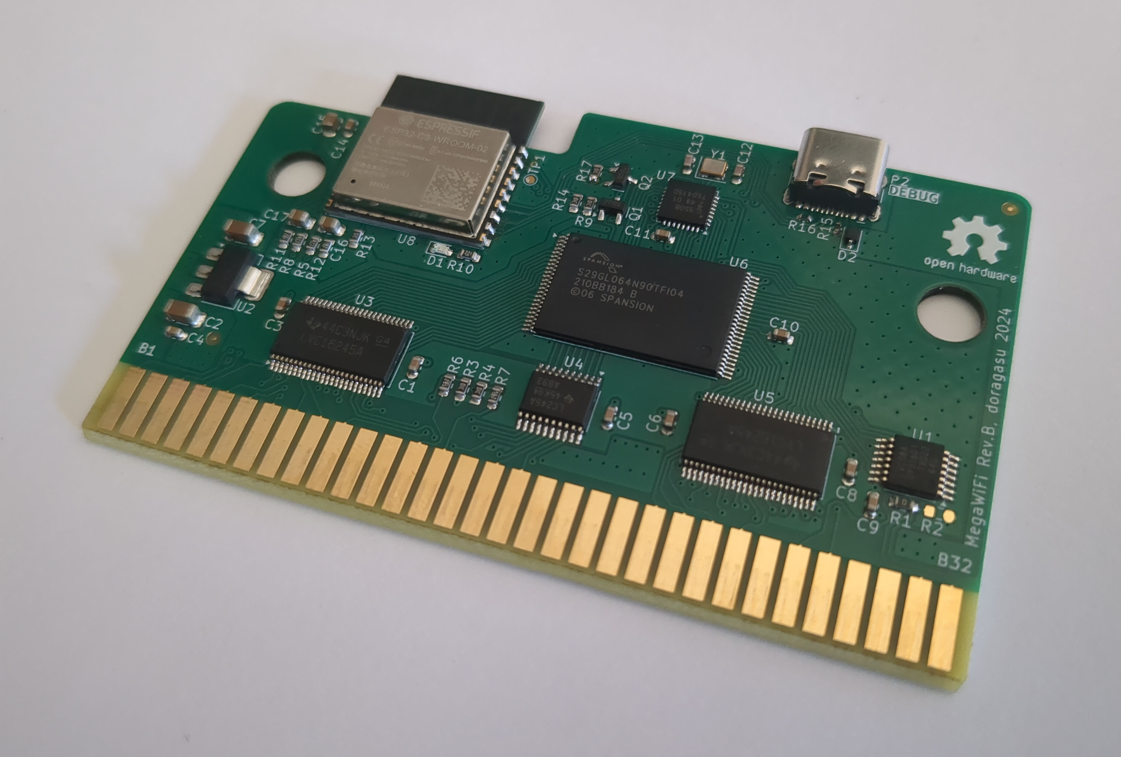
This is the cartridge for the MegaWiFi project. It consists of a cartridge for the SEGA Genesis/Megadrive console, along with a WiFi interface, allowing brave programmers to implement games with online gaming, leaderboards, evil DLCs, etc.
This project was initially created for 1985alternativo, and to this day, as far as I know, only 1985 WorldCup game has used it to implement online play. Will you give it a try?
Have a look to the github project page for more information.
The current cartridge is based on an ESP32-C3 WiFi microcontroller, that has a good specs/price tradeoff. But bear in mind that if needed, it would be easy swapping it for other more powerful ESP32 chip, like for example the ESP32-S3. The current specs are:
Note: The cartridge slashes the the usual 32 megabits maximum of ROM space by implementing a hack: it unmaps the MegaCD and uses its address space. This has the drawback that you cannot access the MegaCD when the hack is enabled. If you need to access the MegaCD, the hack can be disabled, but then the cart is limited to the usual 32 megabits of ROM.
mw-cart is licensed under the CERN OHL 1.2 license. You are free to study, distribute and make modifications to the Documentation, under the aforementioned license terms.
Electronic CAD design files are for KiCAD Open Source electronics design suite. Please install latest version along with KiCAD libraries to open the project. When opening schematic, KiCAD will most likely complain about missing library "doragasu". Despite this warning, the schematic should load nicely (using the cached libraries). To avoid this message, install the missing library and make sure to configure it in the schematic editor.
You can go to the package registry to download artifact packages with the fabrication files, including Gerbers, bill of materials, drawings, CPL file, etc. To get the PCB made, you sould have some knowledge about PCB manufacturing, but I will try to give some indications about how to get the boards made and assembled by JLCPCB.
JLCPCB is a widely known Chinese PCB manufacturer, that can do PCB fabrication and assembly, including component procurement. They are fairly cheap for PCB prototypes and quality is pretty good for boards not having difficult components (such as BGAs with very fine pitch). One of the things that make them have quite competitive pricing, is that they will only assemble components they have stocked. Luckily they source components from LCSC (one of the biggest Chinese suppliers) and have a very wide catalog of components. But even with this wide catalog it is not uncommon that one or more of the components for your board are not available. In this case, they allow you to purchase the components through their platform, and once they receive them, they can be selected for assembly on your boards.
So roughly speaking, the procedure to order assembled PCBs on JLCPCB is as follows:
Getting into the details, the procedure is:
Fab/Manufacturers/mega-wifi-JLCPCB.zip file, that contains the Gerber files, the Fab/Manufacturers/JLCPCB/mega-wifi_bom_jlc.csv that has the BoM (Bill of Materials) and the Fab/Manufacturers/JLCPCB/mega-wifi_cpl_jlc.csv that has the CPL (Component Placement/Centroid) file. We will have to upload these files later.mega-wifi-JLCPCB.zip file we located in step 2. When the files are processed, many board parameters will be populated. Most of the default values will be OK, but some changes are recommended. I will mark with an asterisk (*) the parameters that should be changed from defaults, and will omit some parameters that should be clear enough (like PCB quantity, color, or dimensions that will be automatically obtained from Gerber files):Advanced options defaults should also be OK.
mega-wifi_bom_jlc.csv and mega-wifi_cpl_jlc.csv files we located in step 2. Then click "Process BOM & CPL".Enjoy!
| Qty | Value | Footprint | References |
|---|---|---|---|
| 10 | 100n | Capacitor_SMD:C_0603_1608Metric | C1, C3, C4, C5, C6, C8, C9, C10, C11, C14 |
| 6 | 10k | Resistor_SMD:R_0603_1608Metric | R3, R4, R9, R13, R14, R17 |
| 2 | 12p | Capacitor_SMD:C_0603_1608Metric | C12, C13 |
| 2 | 1u | Capacitor_SMD:C_0805_2012Metric | C16, C17 |
| 2 | 22u | Capacitor_SMD:C_1206_3216Metric | C2, C7 |
| 2 | 2N7002 | Package_TO_SOT_SMD:SOT-23 | Q1, Q2 |
| 2 | 2k2 | Resistor_SMD:R_0603_1608Metric | R11, R12 |
| 2 | 5k1 | Resistor_SMD:R_0402_1005Metric | R15, R16 |
| 2 | 5k6 | Resistor_SMD:R_0603_1608Metric | R6, R7 |
| 2 | 74LVC16245 | Package_SO:TSSOP-48_6.1x12.5mm_P0.5mm | U3, U5 |
| 2 | 8k2 | Resistor_SMD:R_0603_1608Metric | R5, R8 |
| 1 | 0R0 | Resistor_SMD:R_0603_1608Metric | R1 |
| 1 | 10u | Capacitor_SMD:C_0805_2012Metric | C15 |
| 1 | 1M | Resistor_SMD:R_0402_1005Metric | R18 |
| 1 | 1N5819WS | Diode_SMD:D_SOD-323 | D2 |
| 1 | 20 MHz | Crystal:Crystal_SMD_2520-4Pin_2.5x2.0mm | Y1 |
| 1 | 220 | Resistor_SMD:R_0603_1608Metric | R10 |
| 1 | 74LVC08 | Package_SO:TSSOP-14_4.4x5mm_P0.65mm | U1 |
| 1 | 74LVC245 | Package_SO:TSSOP-20_4.4x6.5mm_P0.65mm | U4 |
| 1 | AMS1117-3.3 | Package_TO_SOT_SMD:SOT-223 | U2 |
| 1 | ESP32-C3-WROOM-02 | PCM_Espressif:ESP32-C3-WROOM-02 | U8 |
| 1 | KT-0603R | LED_SMD:LED_0603_1608Metric | D1 |
| 1 | MD-CART-FINGERS | doragasu:MD-CART-FINGERS | P1 |
| 1 | NP | Resistor_SMD:R_0603_1608Metric | R2 |
| 1 | S29GL064N | Package_SO:TSOP-I-48_18.4x12mm_P0.5mm | U6 |
| 1 | TL16C550DRHB | Package_DFN_QFN:Texas_RHB0032E_VQFN-32-1EP_5x5mm_P0.5mm_EP3.45x3.45mm | U7 |
| 1 | TestPoint | TestPoint:TestPoint_Pad_D1.0mm | TP1 |
| 1 | USB_C_Receptacle_USB2.0_16P | Connector_USB:USB_C_Receptacle_HCTL_HC-TYPE-C-16P-01A | P2 |
The 51 most common of 56 parts.

blark/6809sidecar
Experimental daughter board for the Tang Primer 20k Lite


roberto314/EVA-1_Reproduction
Recreation of the very rare K-K Systems EVA-1 Display Adapter for the Epson HX-20 Computer


makerspet/oomwoo-esp32s3-cm
Pi CM4/CM5-compatible Compute Module using ESP32-S3 instead of CPU
It measures 83.8 × 51 mm and has 2 copper layers, 1.6 mm thick.
56 parts, built around the 74LVC16245ADL, 74LVC245AD, ESP32-C3-WROOM-02-H4 and 74LVC08AD. The full list of its parts is on this page, with links to each part's symbol and footprint where PCBKit's library has them.
From the jfryman/mw-cart repository on GitHub, at the commit this page was made from: the board is mega-wifi.kicad_pcb and its schematic mega-wifi.kicad_sch. PCBKit opens the board in the browser, with nothing to install.
Its repository states no licence, so its author keeps all rights: ask jfryman before reusing the design.