2 layers40.1 × 28.3 mm

 jeffqchen/SNES2VGA31
SNES2VGA Dongle for Nintendo Consoles
SNES2VGA is an open-source printed circuit board by jeffqchen, from the jeffqchen/SNES2VGA repository on GitHub, published under the CC-BY-SA-4.0 licence. It is a 2-layer board of 30.8 × 23.6 mm with 17 parts on 23 nets, routed with 121 tracks and 16 vias.
Its parts include 6 capacitors, 5 resistors and 3 connectors. It belongs with the retro computing and games boards of this library.
SNES2VGA Dongle for Nintendo Consoles
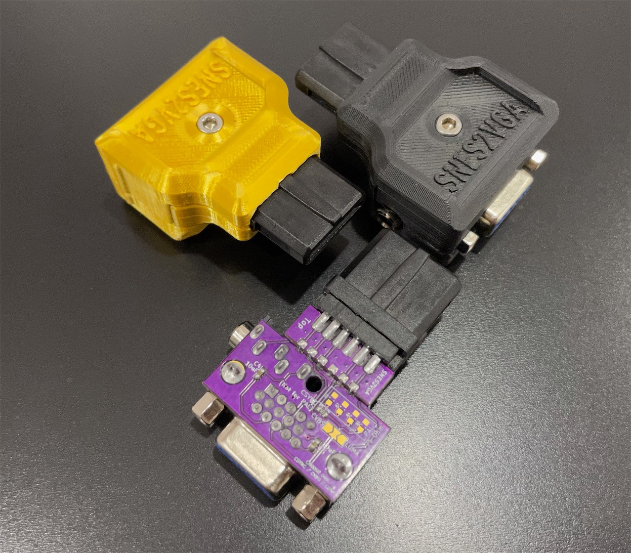
This dongle takes the AV Multi output used on various Nintendo consoles and adapts them into HD15 (VGA), so you can use the commonly available VGA cable for transmitting RGBs video and stereo audio.
Note that consoles usually require RGB mods in order to output RGBs signal.
The NES/Famicom do not generate or output RGB signals natively. They generate composite video and output it as-is or encode it to RF.
For them to output RGB, modding it with an NESRGB and the Nintendo AV Multi style port is required.
(If you installed an 8 or 9-pin MiniDin port, please check my 8DIN2VGA and 9DIN2VGA projects instead.)
No native RGB output. Different models require different levels of modding to restore RGB output (Simple RGB Bypass, N64RGB, etc)
12V on CSync ordeal is still present.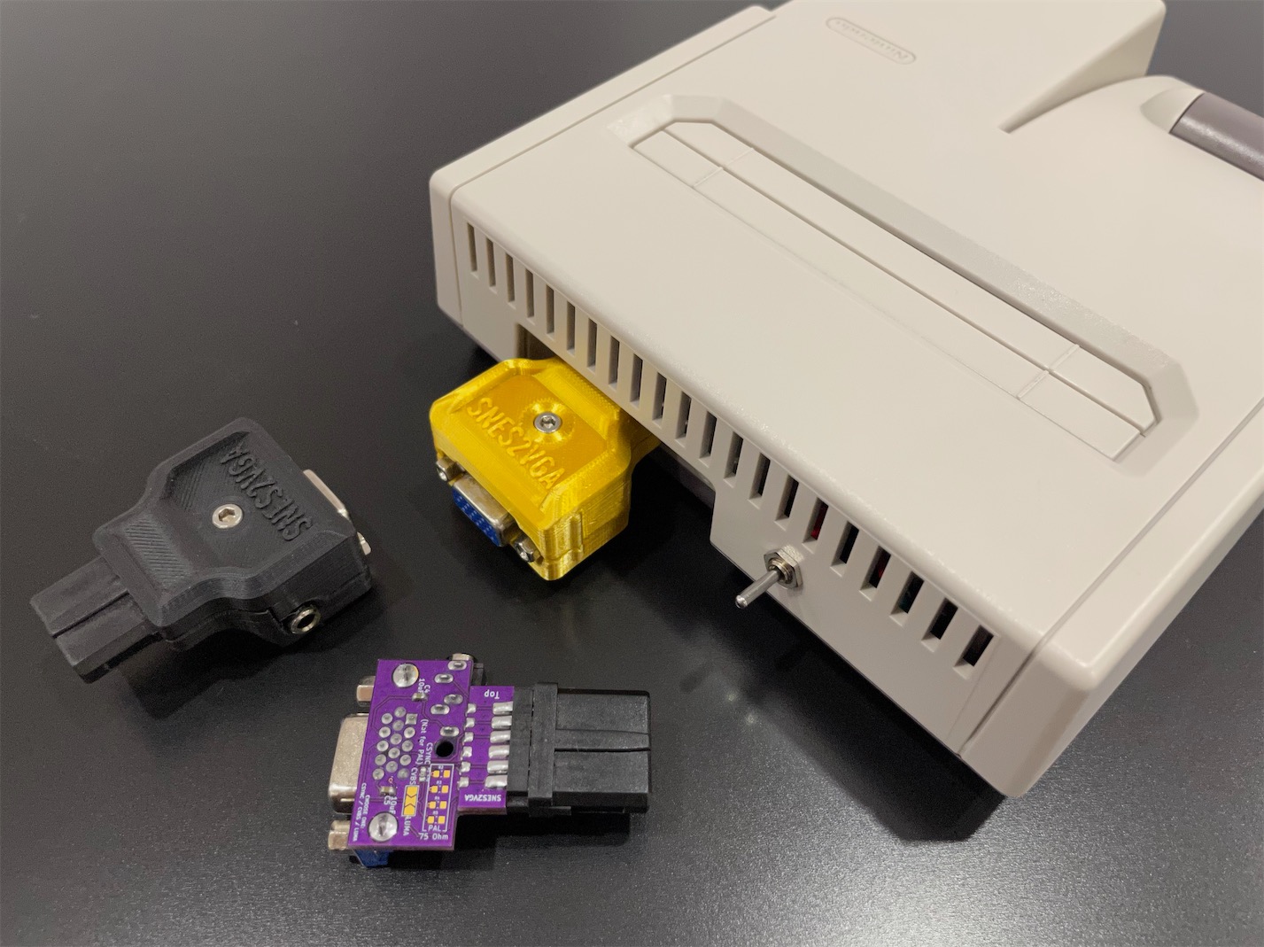
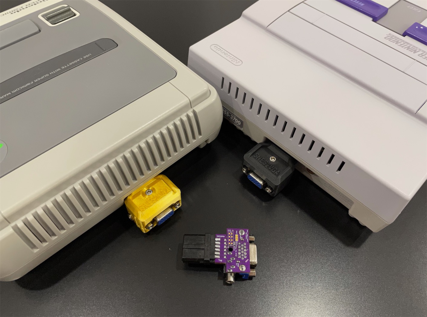
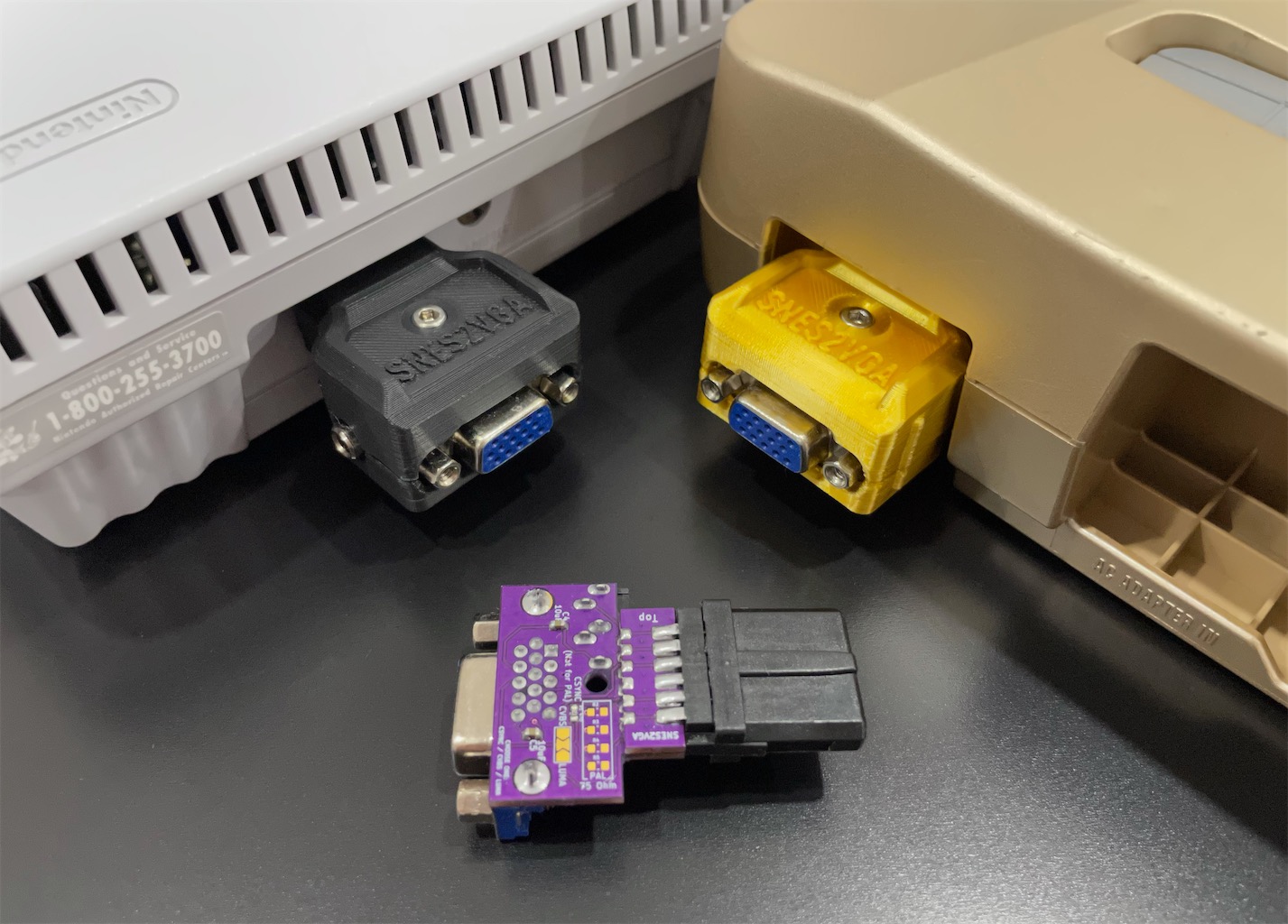
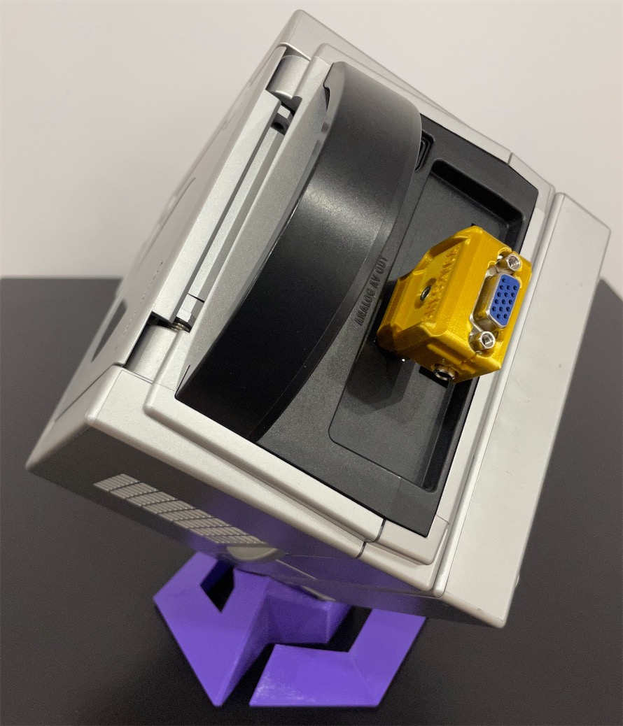
You can choose among CSync, Luma and composite video as your sync signal with the jumper on the PCB.
WARNING: PAL consoles output 12V on the CSync pin. CSync related components should NOT be populated if you are building this dongle for a PAL console.
Audio can be sent within the VGA cable, or broken out from the 3.5mm jack on the dongle. Buzzing may be noticeable when audio is transmitted through the VGA cable in certain scenes in certain games. This is due to insufficient shielding in most VGA cables. If you find the buzzing to be annoying, please use the 3.5mm jack on the dongle for audio outputting. This will ensure the cleanest audio output.
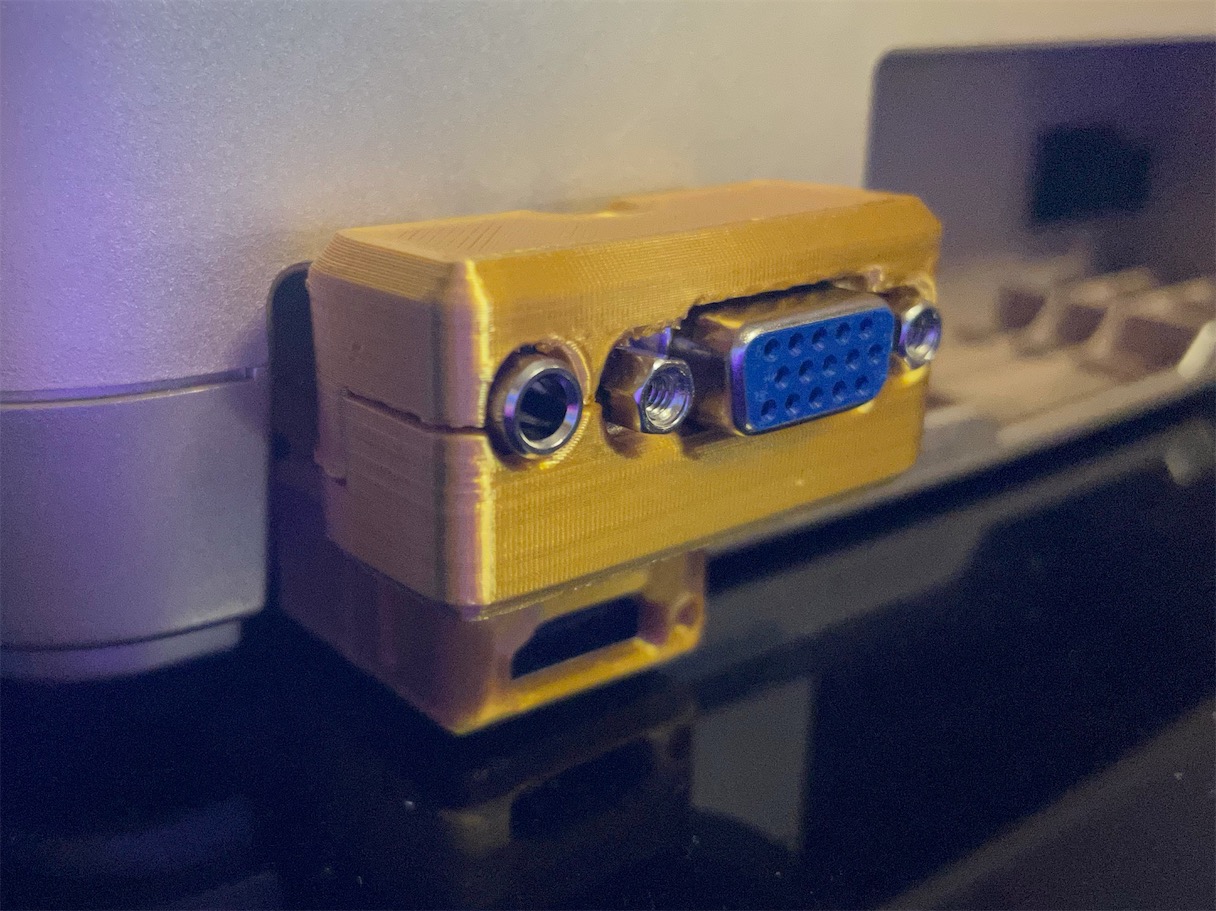
This one works with my N64Digital mini HDMI to Full HDMI Dongle so you could achieve analogue RGBS & digital dual output with full sized plugs without interference.
PCB
Nintendo AV Plug - Link
VGA Port Slim, Female - Link
Vertical 3.5mm Headphone Jack - Link
[1x] M3x20mm screw and nut - Link
[2x] Imperials 0603 SMD Capacitor 6.3V 10uF - C4, C5
3D Printed Shell
Print the files with the split face facing downwards.
Print with support.
For a better mating surface finishing, use raft for bed adhesion.
First, align the sub PCB on top of the main PCB, align with the helper line and make sure the correct sides are facing the outside. Solder the two outside-most castellated pins and pads one by one, making sure the outside of the two boards are flush, so the plug can be soldered properly. Then proceed to solder the rest of the castellated pins to the pads.
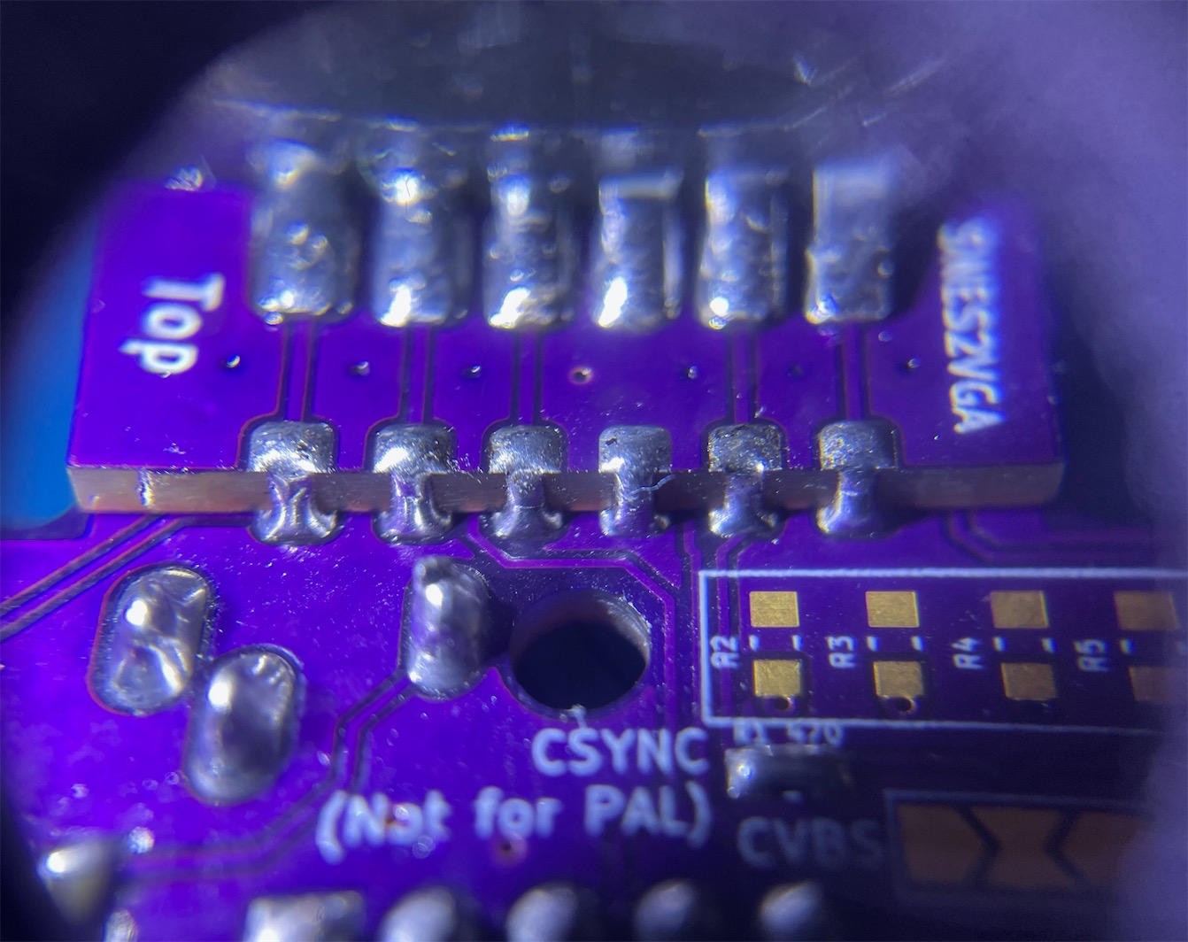
Next, take a Nintendo video plug. Note the pins on the soldering side are sticking out straight. Now bend both rows of the pins inwards, with the help of the edge of a table. This way, the pins will actually be able to touch the pads on the PCB compound.
Tuck the plug onto the compound PCB. Make sure the plug is pointing the correct way up - the notched side of the plug is up, and the side with the smaller sub PCB is up. Align the pins to the pads as good as possible. Make sure there is no gap between the plug and the PCB on the mating edge. Then, solder one pin on each side with a generous amount of solder. Remelt and adjust the position if needed. Then proceed and solder the rest of the pins to the PCB with generous amount of solder.
Solder on the SMD components. Note for NTSC and PAL consoles, the component configurations are quite different. Please follow the instructions on the silk screen.
Solder on the through hole VGA and 3.5mm audio port. Note they are supposed to be on the bottom side of the PCB. Pay attention to the silk screen markings.
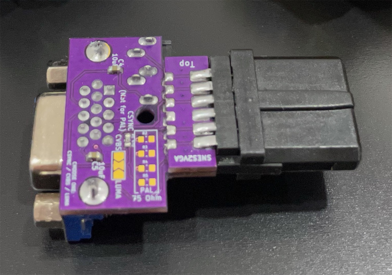
Tuck the assembled PCB into one side of the shell. Make sure the video plug fits correctly in. Then drop the other side of the shell in and slowly bring the two sides to a close. Inspect the shells for any remaining support material if you can't correctly close it up. Finally, put in the screw and nut to secure the whole assembly.
Non-CSync signals are incompatible with the AV3 input on the OSSC. Only TTL CSync works with AV3 on the OSSC.
Mike Chi - Beloved creator of RetroTink
Javier Rodas
Shield: 
This work is licensed under a Creative Commons Attribution-ShareAlike 4.0 International License.

| Qty | Value | Footprint | References |
|---|---|---|---|
| 4 | 100-220uF | SNES2VGA_Library:Cap_SMD_1206 | C1, C2, C3, C6 |
| 4 | 75 | SNES2VGA_Library:Resistor_SMD_0603 | R2, R3, R4, R5 |
| 2 | 10uF | SNES2VGA_Library:Cap_SMD_0603 | C4, C5 |
| 1 | 3.5mm_vertical | SNES2VGA_Library:3.5mm_vertical | J1 |
| 1 | 470 | SNES2VGA_Library:Resistor_SMD_0603 | R1 |
| 1 | AVMulti_Main | SNES2VGA_Library:AV_Multi_Main | P1 |
| 1 | LOGO | SNES2VGA_Library:Outline_PCB_Main | G*** |
| 1 | LUMA_CVBS_SL | SNES2VGA_Library:SolderJumper-3_P1.3mm_Open_RoundedPad1.0x1.5mm | JP1 |
| 1 | NTSC_SYNC | Jumper:SolderJumper-2_P1.3mm_Open_RoundedPad1.0x1.5mm | JP2 |
| 1 | VGA | SNES2VGA_Library:VGA_female_rightangle_slim | P2 |


hoglet67/RGBtoHDMI
Bare-metal Raspberry Pi project that provides pixel-perfect sampling of Retro Computer RGB/YUV video and conversion to HDMI


hackclub/OnBoard
💡 Join 1,000 teenagers and make your first PCB with a $100 grant!

DDeGonge/OS-ARM
This arm is not industrial and it will not be fast, but that is not my goal. But it will hopefully be a very nice looking arm fully capable of 6dof motion, cheap enough to keep it accessable but capable enough to…


It measures 30.8 × 23.6 mm and has 2 copper layers, 1.6 mm thick.
17 parts. The full list of its parts is on this page, with links to each part's symbol and footprint where PCBKit's library has them.
From the jeffqchen/SNES2VGA repository on GitHub, at the commit this page was made from: the board is KiCAD/SNES2VGA/SNES2VGA.kicad_pcb and its schematic KiCAD/SNES2VGA/SNES2VGA.kicad_sch. PCBKit opens the board in the browser, with nothing to install.
Its repository publishes it under the CC-BY-SA-4.0 licence: you may reuse it on that licence's terms (keep the author's notice, and for a copyleft licence share your changes alike).