4 layers100 × 100 mm
Robot
UBC-Thunderbots/Electrical
All things electrical, from radio communication to BLDC motors. Zappity zap!
186 parts3
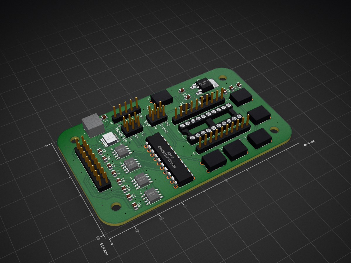
 jdbaptista/MSP-Debugger1
Files for a device that displays instructions stored on an MSP430G2553IN20.
MSP Debugger is an open-source printed circuit board by jdbaptista, from the jdbaptista/MSP-Debugger repository on GitHub. It is a 2-layer board of 86.6 × 51.4 mm with 37 parts on 63 nets, routed with 381 tracks and 86 vias.
It is built around the MSP430G2553IN20, FT230XS-R and AO4882, with the BA033CC0FP-E2, 222ADVBA and 0ZCG0075FF2C among its other parts. Its parts include 10 resistors, 8 ICs, 6 connectors, 6 switches and 4 capacitors. It belongs with the interfaces and adapters boards and the MSP430 boards of this library.


This project is a combination of bare-metal firmware and hardware that displays the assembly instructions stored in the flash memory of an MSP430G2553, specifically the 20 pin DIP package. Please navigate to each section as necessary: Example Operation, Firmware.
The device is shown below and supports the following button interactions:
UP: Move back one instruction. Note that moving back one instruction is equivalent to moving lower in memory because the program counter increments positively each target CPU cycle.
DOWN: Move forward one instruction. Note that moving forward one instruction is equivalent to moving higher in memory because the program counter increments positively each target CPU cycle.
FOLLOW JMP: When the cursor is on a jump instruction, this button moves the cursor to the location specified by the jump. There is also support for following call instructions when the destination operand is an immediate or PC relative offset.
BIN <-> ASM: Switch the display view between machine code (binary), displayed in hexadecimal, and RISC assembly instructions. This button highlights that assembly instructions on the target correspond to variable length machine code due to operand types.
RESET: Move the cursor back to 0xC000, which is the start of code memory. This is implemented by simply resetting the MCU.
USB RESET: Reset the USB to UART bridge. USB data lines are currently in a broken state, so this button does nothing.
The following example code from Texas Instruments is used in this example of the device's operation. The code blinks P1.0 repeatedly. Note that all assembly instructions displayed by the device are confirmed to be correct by Code Composer Studio's professional disassembler.
#include <msp430.h>

void main(void)
{
	WDTCTL = WDTPW | WDTHOLD;		// stop watchdog timer
	P1DIR |= 0x01;					// configure P1.0 as output

	volatile unsigned int i;		// volatile to prevent optimization

	while(1)
	{
		P1OUT ^= 0x01;				// toggle P1.0
		for(i=10000; i>0; i--);     // delay
	}
}
The target is loaded with the assembled machine code for this program and placed in the MSP-Debugger. Unfortunately, the display and USB to UART bridge are currently broken, so an MSP-FET (from any MSP430 development board) is connected to the JTAG header of the debugger. The MSP-FET's backchannel UART to USB bridge is used to convey instructions to the user, operating at 9600 baud with an 8-bit frame, no parity bit, and importantly 2 stop bits (for data integrity). The UART encoding is ISO-8859-1, which is the default in CCS. Immediately after RESET the following instruction are extracted from the target and displayed.
0xC000: SUB.B #2 SP <
0xC002: MOV.B #0x5A80 &0x0120
0xC008: BIS.B #1 &0x0022
0xC00C: XOR.B #1 &0x0021
Using the DOWN button moves the cursor from 0xC000 to 0xC002.
0xC002: MOV.B #0x5A80 &0x0120 <
0xC008: BIS.B #1 &0x0022
0xC00C: XOR.B #1 &0x0021
0xC010: MOV.B #0x2710 0x0000(SP)
An extremely well trained eye will recognize &0x0120 as the location of the WDTCTL register, which can be confirmed by the peripheral file map on page 18 of the MSP430G2x53 Datasheet. Someone without access to the C source code can reference page 363 of the MSP430G2xx User Guide to determine that the value #0x5A80 being moved into WDTCTL register writes the correct watchdog password 0x5A00 (WDTPW) and suspends the watchdog's operation with 0x0080 (WDTHOLD). The watchdog timer will reset the microcontroller if not 'pet' in time by setting WDTCNTCL, so this instruction allows the microcontroller to operate without fear of the watchdog.
Using the BIN <-> ASM button switches the display from assembly to machine code.
0xC002: 0x40B2 0x5A80 0x0120 <
0xC008: 0xD3D2 0x0022
0xC00C: 0xE3D2 0x0021
0xC010: 0x40B1 0x2710 0x0000
In this view it can be seen that the instruction to suspend the watchdog takes 3 words, ie. 48 bits, to encode. This is because the MOV instruction is a double operand instruction type and the opcode 0x40B2 specifies immediate mode for the first operand, which stores the immediate in the second word, and absolute mode for the second operand, which stores its address in the third word. These modes are internally specified by indirect autoincrement mode with the PC register and indexed mode with the SR register, respectively.
The while loop on line 1 should correspond to a jump instruction somewhere in memory, which we navigate forward to discover.
0xC01A: JEQ 0xC00C <
0xC01C: SUB.B #1 0x0000(SP)
0xC020: CMP.B #0 0x0000(SP)
0xC024: JEQ 0xC00C
The first jump instruction found is at 0xC01A, jumping to 0xC00C. This isn't useful in itself because we don't know what was being compared, which was an instruction that was skipped over.
Using the UP button moves the cursor backward by one instruction.
0xC016: CMP.B #0 0x0000(SP) <
0xC01A: JEQ 0xC00C
0xC01C: SUB.B #1 0x0000(SP)
0xC020: CMP.B #0 0x0000(SP)
This instruction is comparing 0 to some variable located at the stack pointer. This should be i from line 12 of the source code because it is the only variable on the stack. Therefore, the jump must correspond to finishing the delay.
Moving the cursor down to the JEQ 0xC00C isntruction and using the FOLLOW JMP instruction brings the cursor to 0xC00C.
0xC00C: XOR.B #1 &0x0021 <
0xC010: MOV.B #0x2710 0x0000(SP)
0xC016: CMP.B #0 0x0000(SP)
0xC01A: JEQ 0xC00C
Finally, it is seen that this XOR instruction corresponds to toggling P1.0, as it is the first thing to occur within the while loop!
An MSP430G2553, aside from being the target type, is also used as the main microcontroller for the device. Firmware was developed using register level C programming in Code Composer Studio. Development followed information derived from the MSP430G2xx User Guide, the MSP430G2x53 Datasheet, and the MSP430 JTAG Programming Guide. Three libraries were developed to handle separate facets of the project requirements:
UART Driver: This library handles control of the USCI peripheral to communicate via the UART module. This driver handles configuration of USCI and UART registers, buffering of user printing output, and transmission with a builtin interrupt handler. The driver offers a user-friendly API (ex. wait_print(char *input) and uart_print_hex(uint16_t input)) optimized for spaced calls. The wait_print function is most likely to be used, and currently implements polling until the previous message is finished being sent.
JTAG Driver: This library handles interfacing with the target through its JTAG debugging interface. Internally, the interface is implemented as an FSM that is controlled by five input and output lines: TDI, TDO, TMS, TCK, and TEST. This driver works by bit banging the correct FSM sequences on GPIO pins. The API offers a variety of functions (specified by the JTAG Programming Guide), but the most important for this project is readMem(uint16_t address). This function returns the value stored in the target at a particular memory address.
Disassembler: This library handles conversion of machine code to RISC assembly instruction. Information about the representation of each instruction as machine code can be found in the MSP430G2xx User Guide, specifically the CPU section. The MSP430G2553 contains a 16-bit CPU supporting variable length instructions ranging from a minimum of 1 word to a maximum of 3 words. This presented a significant design challenge as moving one assembly instruction backward is ambiguously a shift of 1, 2, or 3 words in memory with little to hint at which is correct. This ambiguity stems from the various addressing modes (ex. indexed mode) and instruction types (ex. single operand). The disassembler has no remedy to this issue; rather, it is currently solved by the main program which simply begins from the beginning of flash memory and iterates forward until finding the correct instruction. It is planned to speed up this process with a significantly sized cache of nearby instruction locations.
The main program handles user button input with interrupts on the corresponding GPIO pins and a simple button debounce system using the timer peripheral. The program enters LPM3 while waiting for user input, with the timer running on ACLK sourced from the 12kHz VLO waking the program up if a button debounce has finished.
| Qty | Value | Footprint | References |
|---|---|---|---|
| 10 | 10K | Capacitor_SMD:C_0805_2012Metric | R1, R2, R3, R4, R5, R6, R7, R8, R9, R10 |
| 6 | 222ADVBA | buttons:SW_222ADVBA | SW1, SW2, SW3, SW4, SW5, SW6 |
| 4 | AO4882 | project:SO-8_AOS | U5, U6, U7, U8 |
| 2 | 10uF | Capacitor_SMD:C_0805_2012Metric | C3, C4 |
| 2 | Conn_01x10 | Connector_PinHeader_2.54mm:PinHeader_1x10_P2.54mm_Vertical | J6, J7 |
| 1 | 0.1uF | Capacitor_SMD:C_0805_2012Metric | C1 |
| 1 | 0ZCG0075FF2C | Fuse:Fuse_1812_4532Metric | F1 |
| 1 | 10K | project:TRIM_3362P-1-103LF | VR1 |
| 1 | 1uF | Capacitor_SMD:C_0805_2012Metric | C2 |
| 1 | BA033CC0FP-E2 | digikey-footprints:TO-252-3 | U3 |
| 1 | Conn_02x10 | project:DIL_CONN_110-83-320-41-001101 | J2 |
| 1 | FT230XS-R | project:SOIC_30XS-R_FTD | U4 |
| 1 | MSP430G2553IN20 | Package_DIP:DIP-20_W7.62mm | U1 |
| 1 | MSP_FET PORT | Connector_PinHeader_2.54mm:PinHeader_2x03_P2.54mm_Vertical | J4 |
| 1 | SS14HE3_B/H | Diode_SMD:D_SMA | D1 |
| 1 | USB JUMPER | Connector_PinHeader_2.54mm:PinHeader_2x03_P2.54mm_Vertical | J5 |
| 1 | USB_B_Micro | Connector_PinHeader_2.54mm:PinHeader_1x05_P2.54mm_Vertical | J1 |
| 1 | ~ | Connector_PinHeader_2.54mm:PinHeader_2x09_P2.54mm_Vertical | U2 |
It measures 86.6 × 51.4 mm and has 2 copper layers, 1.6 mm thick.
37 parts, built around the MSP430G2553IN20, FT230XS-R, AO4882 and BA033CC0FP-E2. The full list of its parts is on this page, with links to each part's symbol and footprint where PCBKit's library has them.
From the jdbaptista/MSP-Debugger repository on GitHub, at the commit this page was made from: the board is Hardware/msp-debugger/msp-debugger.kicad_pcb and its schematic Hardware/msp-debugger/msp-debugger-con.kicad_sch. PCBKit opens the board in the browser, with nothing to install.
Its repository states no licence, so its author keeps all rights: ask jdbaptista before reusing the design.
UBC-Thunderbots/Electrical
All things electrical, from radio communication to BLDC motors. Zappity zap!


daniel-bornhorst/GVH-ALY-PM-InteractiveCounter
GVH Alley Bar - Prime Materia - Interactive Cap Touch Countertop

fabiansteiner/OpenValve
3D-printable pinch valve for irrigation and sensor-driven liquid control.

KeioRoboticsAssociation/SpringRobocon2026_mainboard
関東春ロボコン2026のメイン基板です


