2 layers19 × 76 mm
Sub
google/mozc-devices
Circuit diagrams and firmware source code for Gboard DIY keyboards
15 parts3kApache-2.0

 jcfurey/can_cap_boards
A repo to contain different PCBs with associated gerber files and SPICE sim docs.
Princeton reverb aa1164 is an open-source printed circuit board by jcfurey, from the jcfurey/can_cap_boards repository on GitHub, published under the Apache-2.0 licence. It is a 2-layer board of 60 × 54 mm with 15 parts on 7 nets, routed with 8 tracks and 0 vias.
Its parts include 6 connectors, 4 capacitors and 2 resistors.
KiCad 7 project for the Princeton Reverb (AA1164) filter-cap board. This is a starting point: electrically complete, ERC/DRC-clean, with the HV creepage and split-ground rules baked in — but the placement and mechanical fit still want a pass in the GUI before you fab it.
Built/validated with KiCad 7.0.11. KiCad 9 opens it fine (it will offer to upgrade the files). The two generator scripts below are the scaffolding used to create it; the
.kicad_sch/.kicad_pcbare now the editable sources.
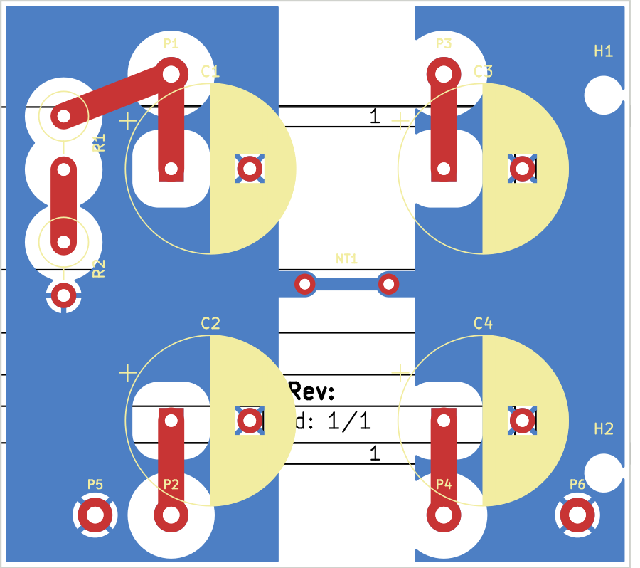
B.Cu split ground pours (blue) joined only at the NT1 star-tie; F.Cu B+ traces (red); 2×2 caps with each B+ wire-entry beside its cap; bleeder R1/R2 top-left; mounting holes right. The wide white rings are the 2.5 mm HV anti-pads in the pour.
| File | What |
|---|---|
princeton_reverb_aa1164.kicad_pro | Project (net classes: 2.5 mm clearance / 2.5 mm tracks) |
princeton_reverb_aa1164.kicad_sch | Schematic — 4 caps, bleeder, 6 wire-entry pads, star-tie, 2 mounts |
princeton_reverb_aa1164.kicad_pcb | 2-layer board: B+ on F.Cu, split GND pours on B.Cu |
wire_entry.pretty/ | Custom footprints: WireEntry_BPlus, WireEntry_GND (1.6 mm hole / 3.3 mm pad), StarTie_8mm (net-tie) |
fp-lib-table / sym-lib-table | Register the project footprint library |
generate_sch.py / generate_pcb.py | The scripts that generated the above (kiutils + pcbnew) |
fab/ | Fabrication outputs — see fab/ |
drc.rpt | Saved DRC run (0 errors) |
HV_A..HV_D (each = wire-entry pad + cap "+",
plus the bleeder on A) — they only join outside the board, in the amp.BLEED_MID is the junction of the two series bleeder resistors.GND-PWR (caps A·B + bleeder) and GND-PRE
(caps C·D), joined only at the NT1 star-tie (a net-tie footprint, so DRC
permits the single intentional short). Omit/DNP NT1 to run dual returns.lib_footprint_issues (8) — headless DRC has no global footprint-library
table; these disappear in the GUI.silk_over_copper (4) — cosmetic cap-outline silk over mask openings.kicad-cli has no erc/drc subcommand (KiCad 8+), so ERC/DRC were
run via the netlist export and pcbnew.WriteDRCReport. Re-run ERC and DRC in
your GUI as a final check after any edits.This was placed/routed blind to the real chassis. In the GUI:
CP_Radial_D16.0mm_P7.50mm
(sized for the 47 µF); the 22/33 µF bodies are smaller, so swap to the right
case once you pick exact parts.pip install kiutils
python3 generate_sch.py # writes the .kicad_sch
python3 generate_pcb.py # writes the .kicad_pcb, fills zones, runs DRCRegenerating overwrites GUI edits — once you start editing in KiCad, treat the
.kicad_sch/.kicad_pcb as the sources and retire the scripts.
| Qty | Value | Footprint | References |
|---|---|---|---|
| 2 | MountingHole:MountingHole_3.2mm_M3 | H1, H2 | |
| 2 | 100k | Resistor_THT:R_Axial_DIN0414_L11.9mm_D4.5mm_P5.08mm_Vertical | R1, R2 |
| 2 | 22uF | Capacitor_THT:CP_Radial_D16.0mm_P7.50mm | C2, C3 |
| 1 | 33uF | Capacitor_THT:CP_Radial_D16.0mm_P7.50mm | C4 |
| 1 | 47uF | Capacitor_THT:CP_Radial_D16.0mm_P7.50mm | C1 |
| 1 | B+1_A | wire_entry:WireEntry_BPlus | P1 |
| 1 | B+2_B | wire_entry:WireEntry_BPlus | P2 |
| 1 | B+3_C | wire_entry:WireEntry_BPlus | P3 |
| 1 | B+4_D | wire_entry:WireEntry_BPlus | P4 |
| 1 | GND-PRE | wire_entry:WireEntry_GND | P6 |
| 1 | GND-PWR | wire_entry:WireEntry_GND | P5 |
| 1 | STAR | wire_entry:StarTie_8mm | NT1 |
google/mozc-devices
Circuit diagrams and firmware source code for Gboard DIY keyboards

hoglet67/RGBtoHDMI
Bare-metal Raspberry Pi project that provides pixel-perfect sampling of Retro Computer RGB/YUV video and conversion to HDMI

mntmn/amiga2000-gfxcard
MNT VA2000, an Open Source Amiga 2/3/4000 Graphics Card (Zorro II/III), written in Verilog

hackclub/OnBoard
💡 Join 1,000 teenagers and make your first PCB with a $100 grant!

kenp-io/not-for-airpods-repairs
The content of this repository is licensed under the WTFPL License. Please have a close look at the terms before using this material.

Luos-io/luos_engine
Open-source and real-time orchestrator for cyber-physical-systems, to easily design, test and deploy embedded applications and digital twins.

Chrismettal/EleLab_v2
Cheap DIY lab system for hobbyists and the tinkering folk

It measures 60 × 54 mm and has 2 copper layers, 1.6 mm thick.
15 parts. The full list of its parts is on this page, with links to each part's symbol and footprint where PCBKit's library has them.
From the jcfurey/can_cap_boards repository on GitHub, at the commit this page was made from: the board is princeton_reverb_aa1164/kicad/princeton_reverb_aa1164.kicad_pcb and its schematic princeton_reverb_aa1164/kicad/princeton_reverb_aa1164.kicad_sch. PCBKit opens the board in the browser, with nothing to install.
Its repository publishes it under the Apache-2.0 licence: you may reuse it on that licence's terms (keep the author's notice, and for a copyleft licence share your changes alike).