2 layers24 × 16 mm

 JBlitzar/dapt
usb adapters
Dapt is an open-source printed circuit board by JBlitzar, from the JBlitzar/dapt repository on GitHub, published under the GPL-3.0 licence. It is a 2-layer board of 64 × 109.5 mm with 42 parts on 82 nets, routed with 487 tracks and 42 vias.
It is built around the MF1/4W-5.1KΩ±1%T52, GT-USB-7035A and AM90, with the MC-337 and USB3150-30-130-A among its other parts.


So looking at the bom, you can see that it's super expensive, like $50. You might be thinking, "what's going on there? I thought this project was explicitly focused on being low-cost!"
There are a few points I'd like to preempt.
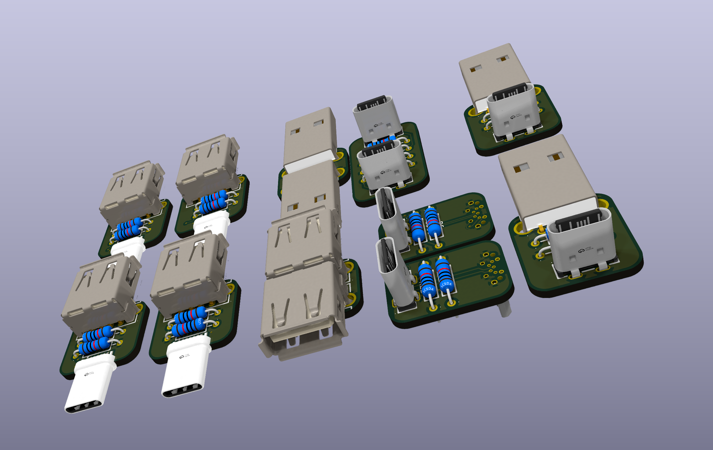
There are no other enclosures, so this is the 3D model too. A STEP export is at dapt.step
dapt is a family of USB adapters.
There are some opinionated choices that were made:
I made dapt because I wanted some dead-simple USB adapters, and I thought it'd be a fun project.
Current adapters:
| Variant | Schematic |
|---|---|
| A female to A female | 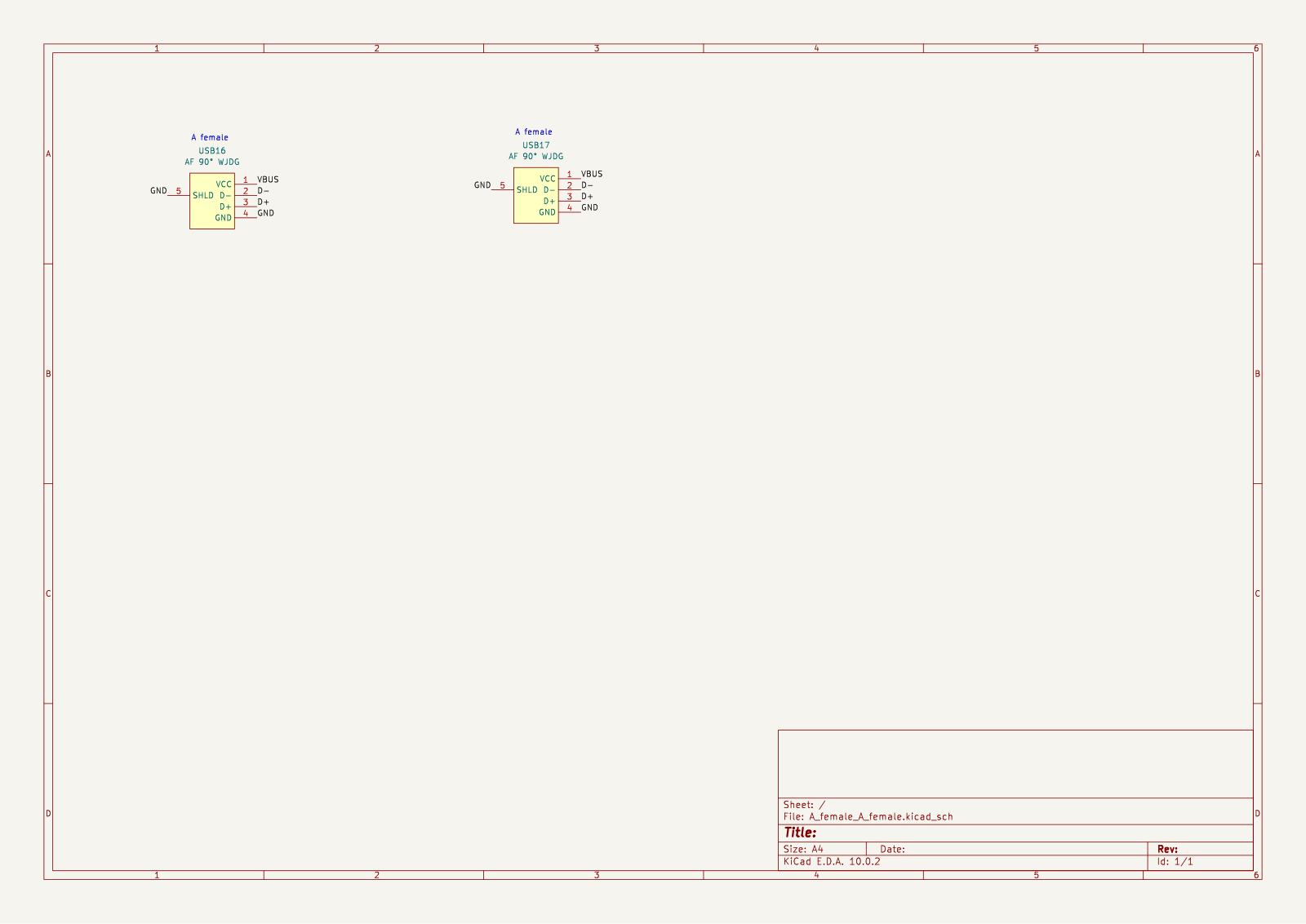 |
| A female to C male | 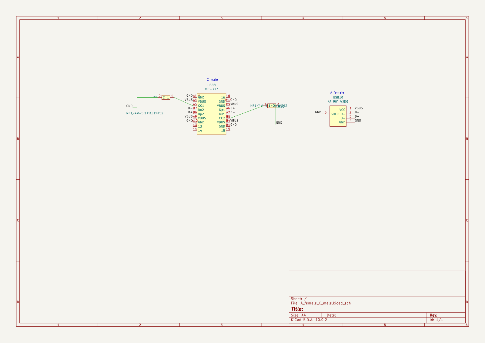 |
| A male to A male | 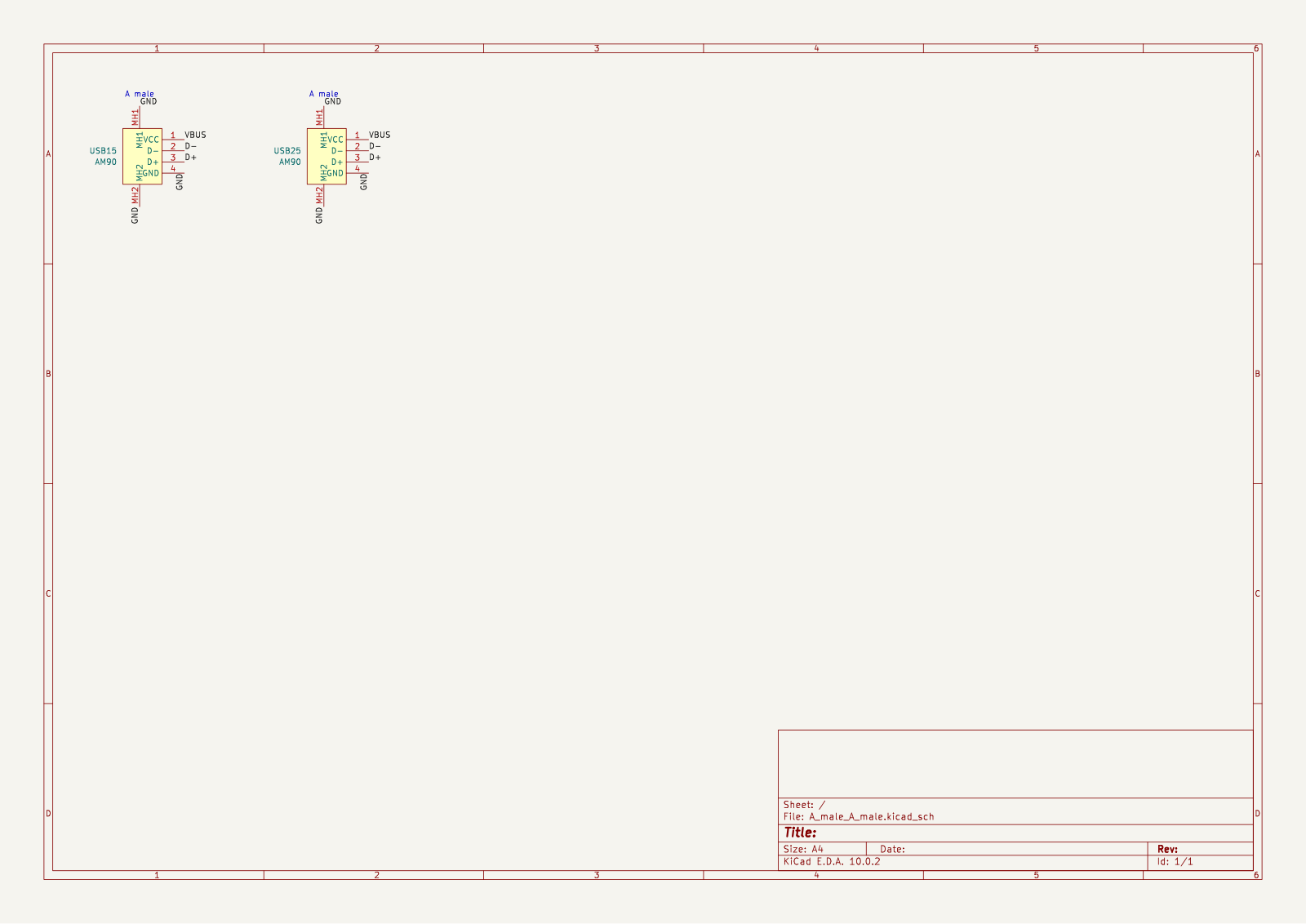 |
| A male to C female | 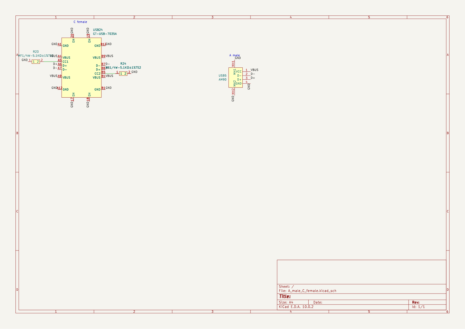 |
| C female to C female | 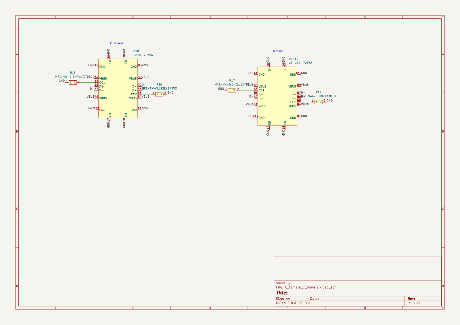 |
| C female to micro male | 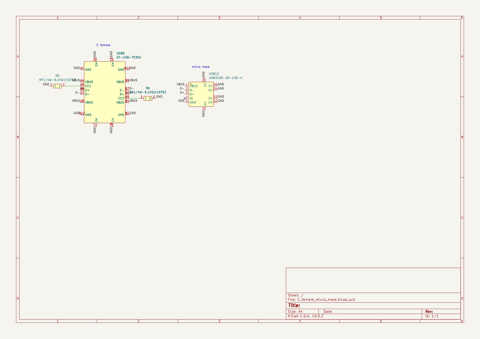 |
| Variant | Front | Back |
|---|---|---|
| A female to A female | 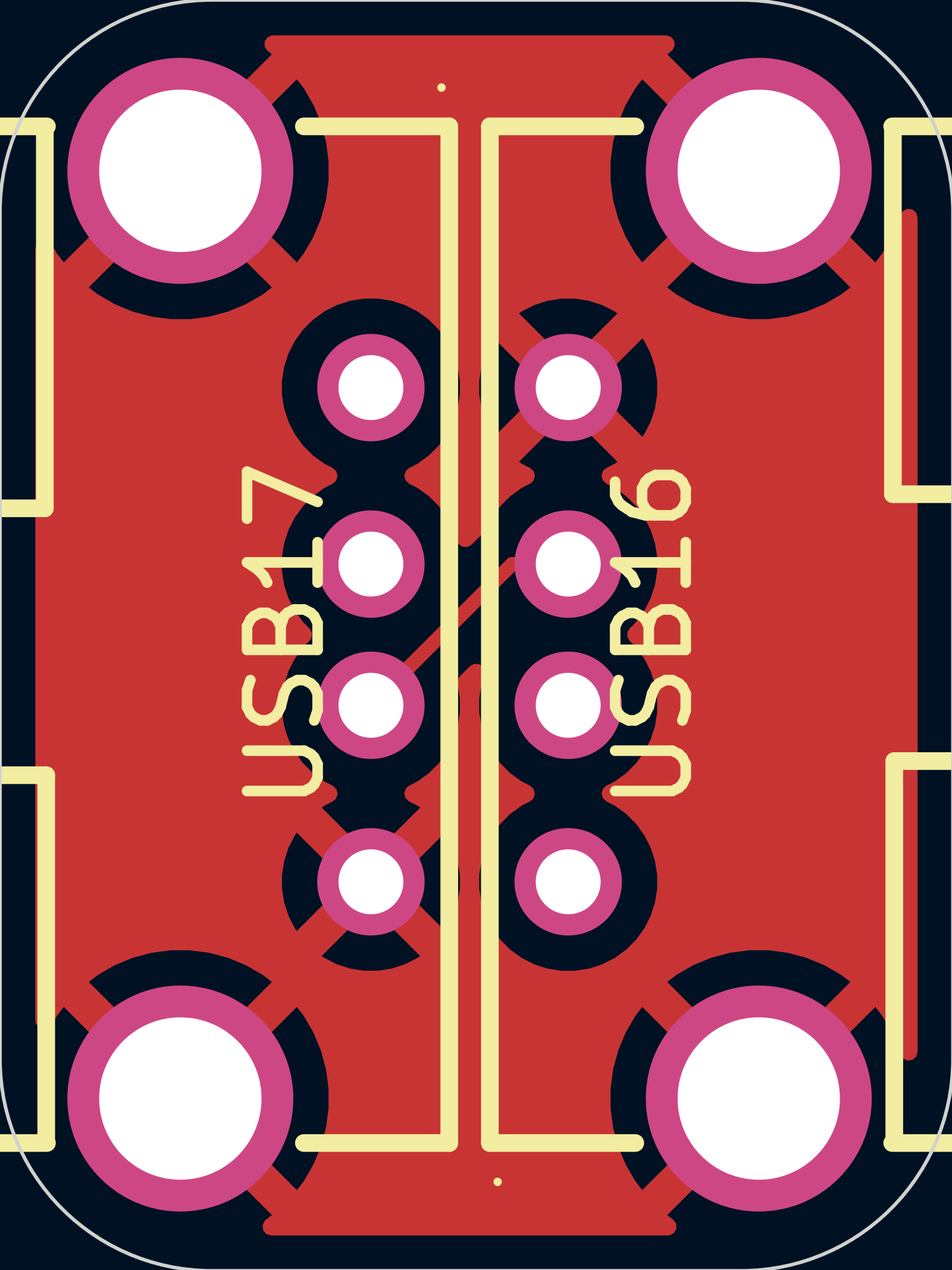 |  |
| A female to C male | 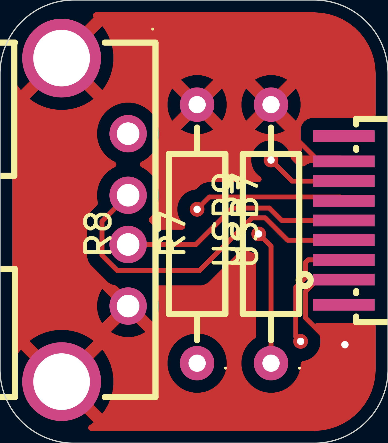 |  |
| A male to A male | 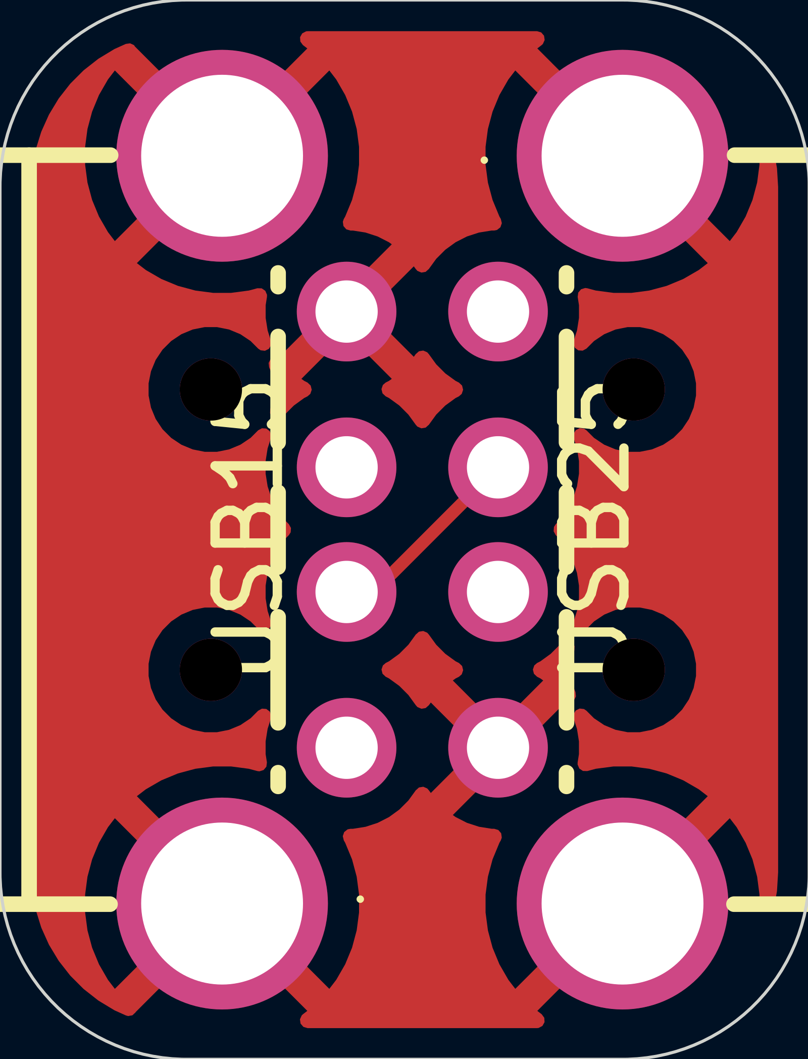 | 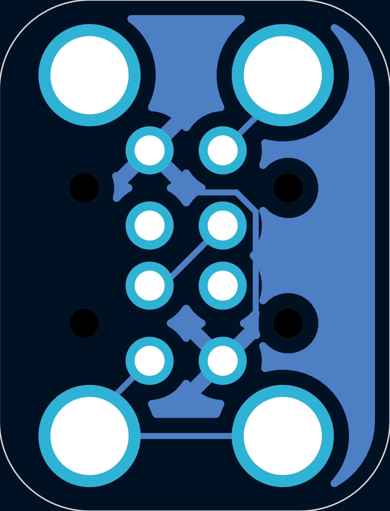 |
| A male to C female | 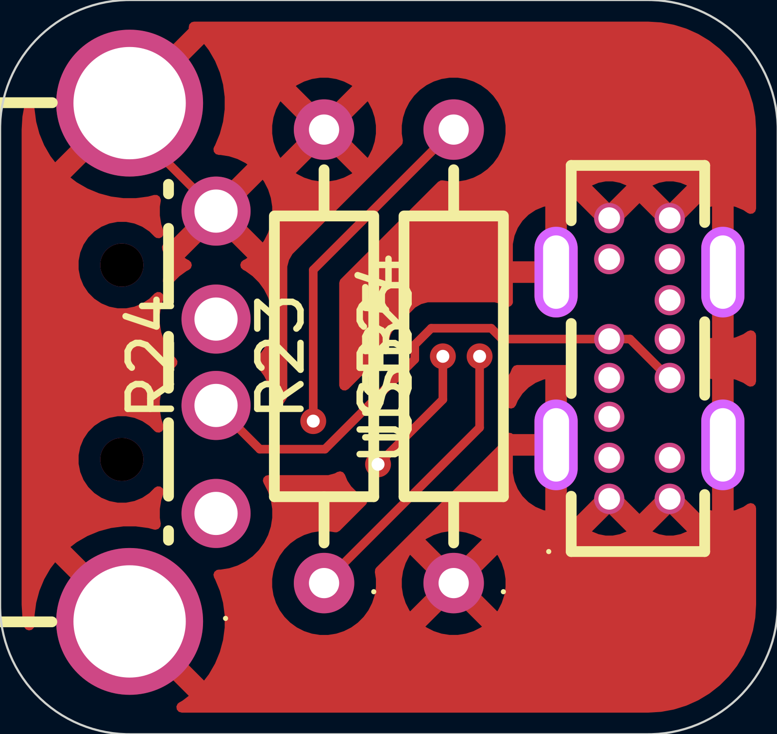 | 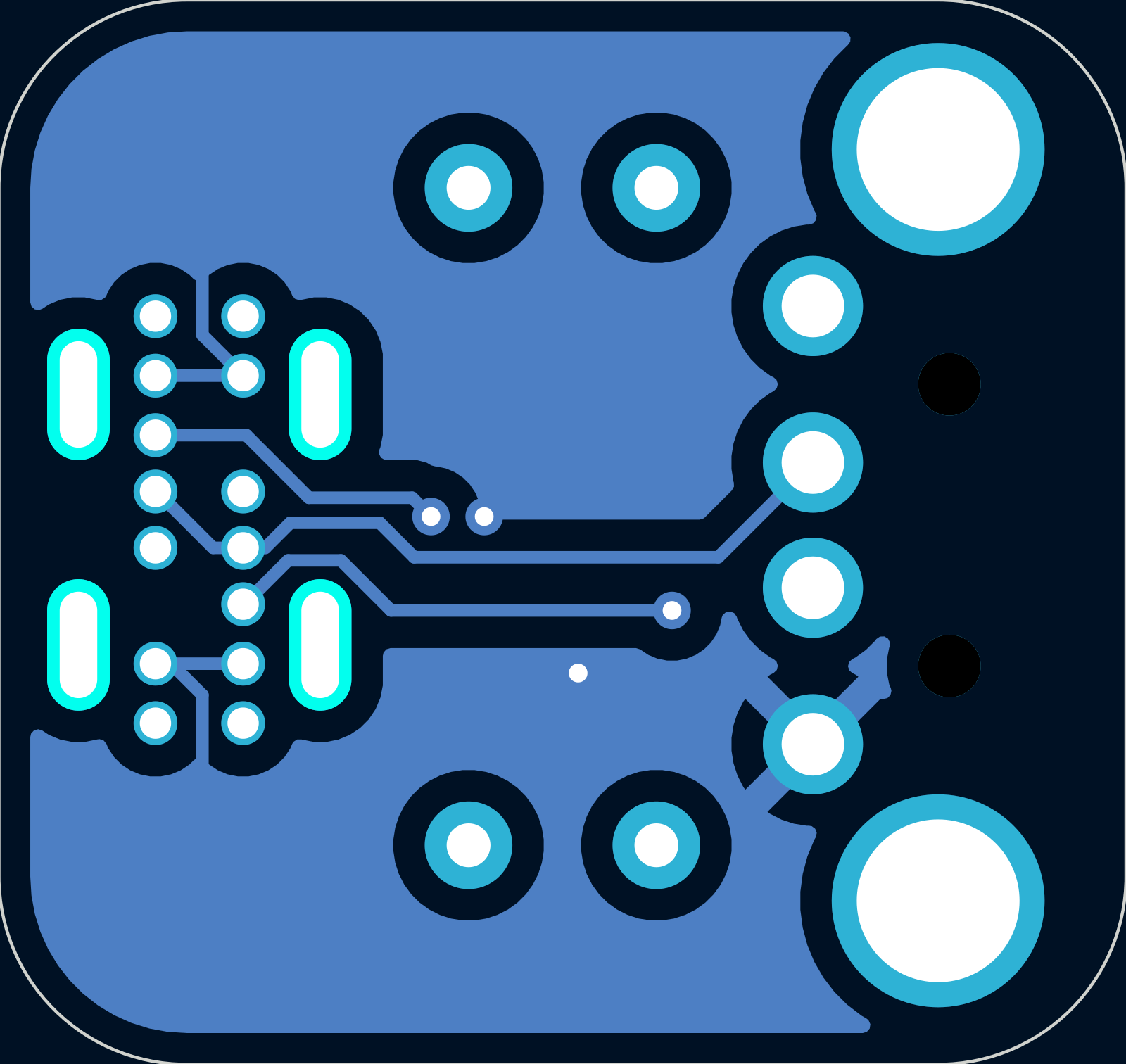 |
| C female to C female | 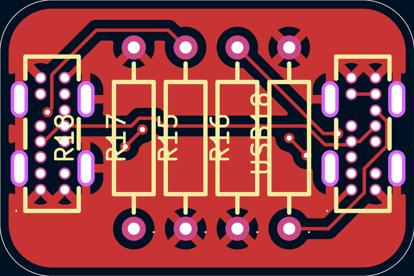 | 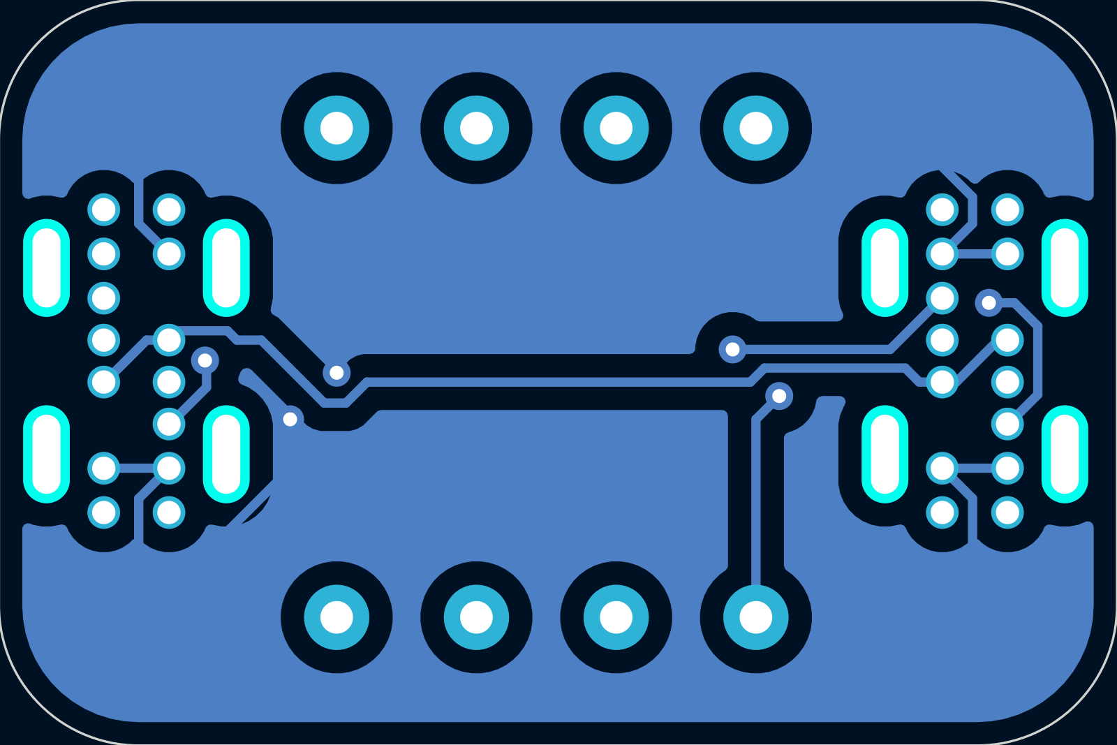 |
| C female to micro male | 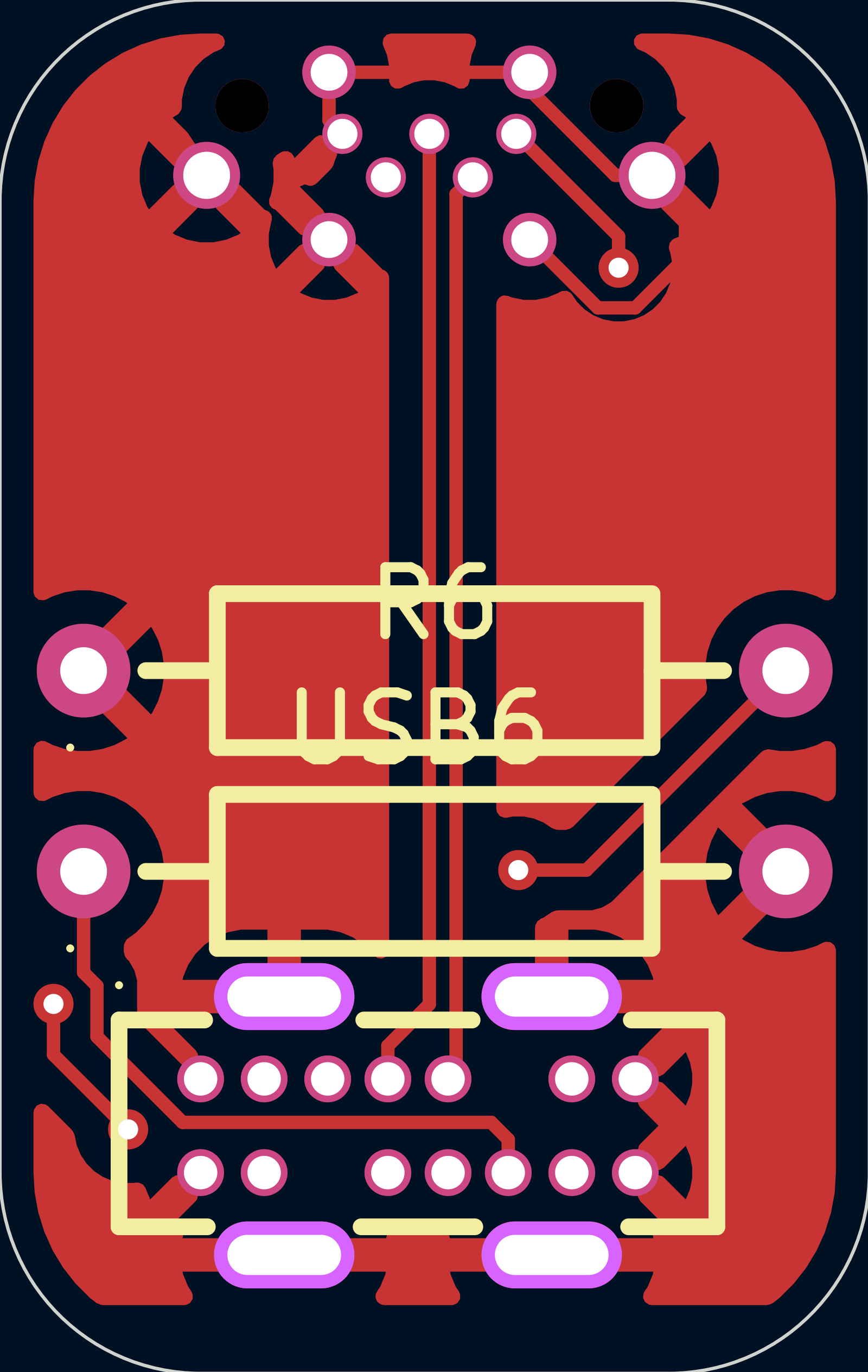 | 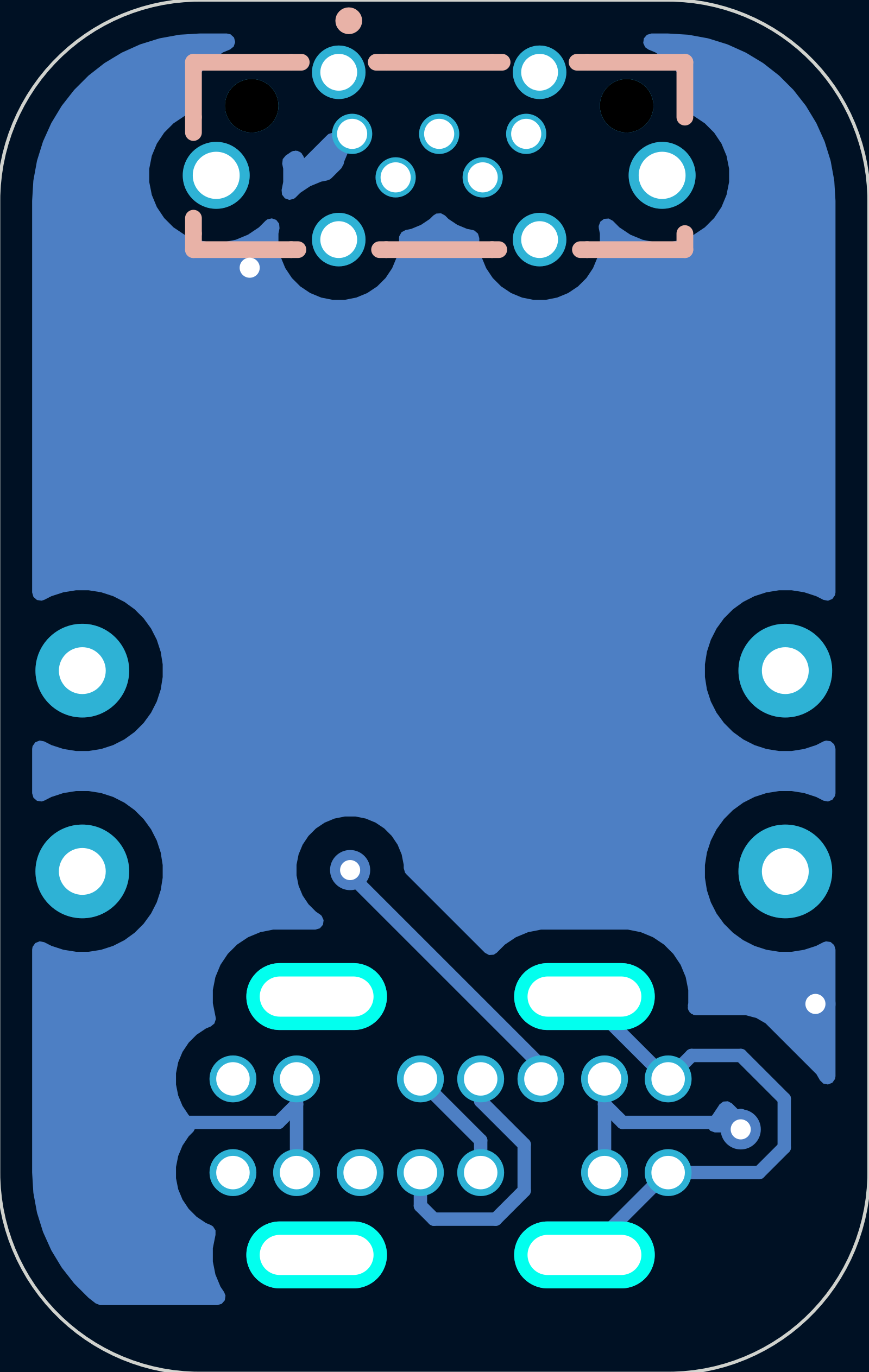 |
in PCB/exported_variants/gerbers. A bit unique because this is multiple boards/variants in one.
Please see the about cost section.
| Item | link | qty | extended price | notes |
|---|---|---|---|---|
| C male A female board | N/A | 20 | 5.1 | |
| A male A male board | N/A | 5 | 4.2 | |
| C female C female board | N/A | 5 | 2.1 | |
| A male C female board | N/A | 10 | 5.2 | |
| C female micro male board | N/A | 10 | 5.5 | |
| USB A male | https://www.lcsc.com/product-detail/C404965.html?s_z=n_q_C404965&globalKeyword=C404965 | 15 | 1.33 | |
| USB A female | https://www.lcsc.com/product-detail/C456018.html?s_z=n_q_C456018&globalKeyword=C456018 | 20 | 0.97 | |
| USB C male | https://www.lcsc.com/product-detail/C22355747.html?s_z=n_q_C22355747&globalKeyword=C22355747 | 20 | 5.85 | |
| USB C female | https://www.lcsc.com/product-detail/C22384780.html?s_z=n_q_C22384780&globalKeyword=C22384780 | 30 | 8.53 | |
| micro male | https://www.lcsc.com/product-detail/C7407276.html?s_z=n_q_C7407276&globalKeyword=C7407276 | 10 | 11.75 | |
| lcsc + jlc shipping | N/A | 1 | 0 | shipping free bc imma order it with other stuff |
| total | N/A | 1 | 50.53 |
| Qty | Value | Footprint | References |
|---|---|---|---|
| 20 | MF1/4W-5.1KΩ±1%T52 | easyeda2kicad:RES-TH_BD2.3-L6.5-P10.50-D0.5 | R5, R10, R11, R12, R13, R14, R15, R16, R17, R18, R19, R20, R21, R22, R23, R24 +4 |
| 6 | AF 90° WJDG | easyeda2kicad:USB-A-TH_AF-WJDG | USB9, USB10, USB13, USB16, USB17, USB21 |
| 6 | GT-USB-7035A | easyeda2kicad:TYPE-C-TH_GT-USB-7035A | USB6, USB14, USB18, USB19, USB22, USB24 |
| 4 | AM90 | easyeda2kicad:USB-AM-TH_AM90 | USB4, USB5, USB15, USB25 |
| 4 | MC-337 | easyeda2kicad:USB-C-SMD_14P-P0.80_MC-337 | USB7, USB8, USB11, USB20 |
| 2 | USB3150-30-130-A | easyeda2kicad:USB-B-TH_USB3150-30-130-A | USB12, USB23 |
It measures 64 × 109.5 mm and has 2 copper layers, 1.6 mm thick.
42 parts, built around the MF1/4W-5.1KΩ±1%T52, GT-USB-7035A, AM90 and MC-337. The full list of its parts is on this page, with links to each part's symbol and footprint where PCBKit's library has them.
From the JBlitzar/dapt repository on GitHub, at the commit this page was made from: the board is PCB/dapt/dapt.kicad_pcb and its schematic PCB/dapt/A_female_A_female.kicad_sch. PCBKit opens the board in the browser, with nothing to install.
Its repository publishes it under the GPL-3.0 licence: you may reuse it on that licence's terms (keep the author's notice, and for a copyleft licence share your changes alike).


performance-tuned/sd-net-2.0
Open-source full-size USB SD card reader (GL823K). CERN-OHL-S-2.0.


owhite/balancing-robot-notes
A control theory and software development repo for a balancing robot.

rusefi/rusefi
rusefi - GPL internal combustion engine control unit
