2 layers66.9 × 74.5 mm
 javinwittig/Hackpad1
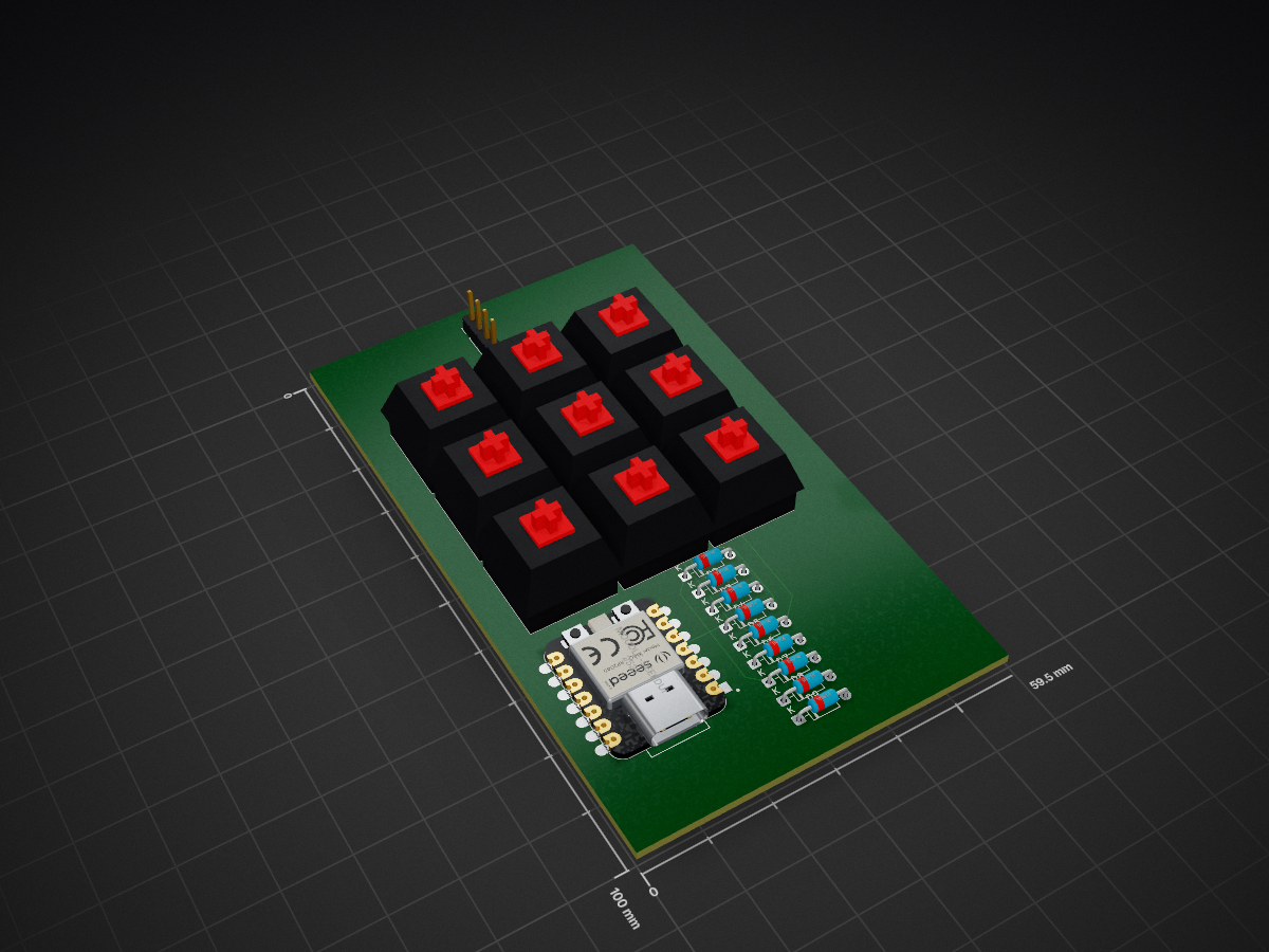
I made a custom 9-key macropad in a 3×3 layout, built with a Seeed Studio XIAO (SAMD21). Each switch has its own diode, wired as a 3×3 key matrix. It also features a small OLED display.
Schaltplatte 6 Tasten is an open-source printed circuit board by javinwittig, from the javinwittig/Hackpad repository on GitHub. It is a 2-layer board of 59.5 × 100 mm with 20 parts on 23 nets, routed with 164 tracks and 0 vias.
Its parts include 9 diodes, 9 switches, 1 IC and 1 connector. It belongs with the lEDs and displays boards of this library.
I made a custom 9-key macropad in a 3×3 layout, built with a Seeed Studio XIAO (SAMD21). Each switch has its own diode, wired as a 3×3 key matrix. It also features a small OLED display.
| Folder | Contents |
|---|---|
Assets/ | Renders/photos used in this README (schematic, PCB, case) |
CAD/ | 3D assembly model (Assembly1.0.step) |
Firmware/ | code.py (KMK firmware source) and a compiled .hex build |
pcb/ | KiCad project (schematic + PCB layout, .kicad_pro/.kicad_sch/.kicad_pcb) |
Production/ | Manufacturing-ready files: case top/bottom (.step) and PCB gerbers.zip |
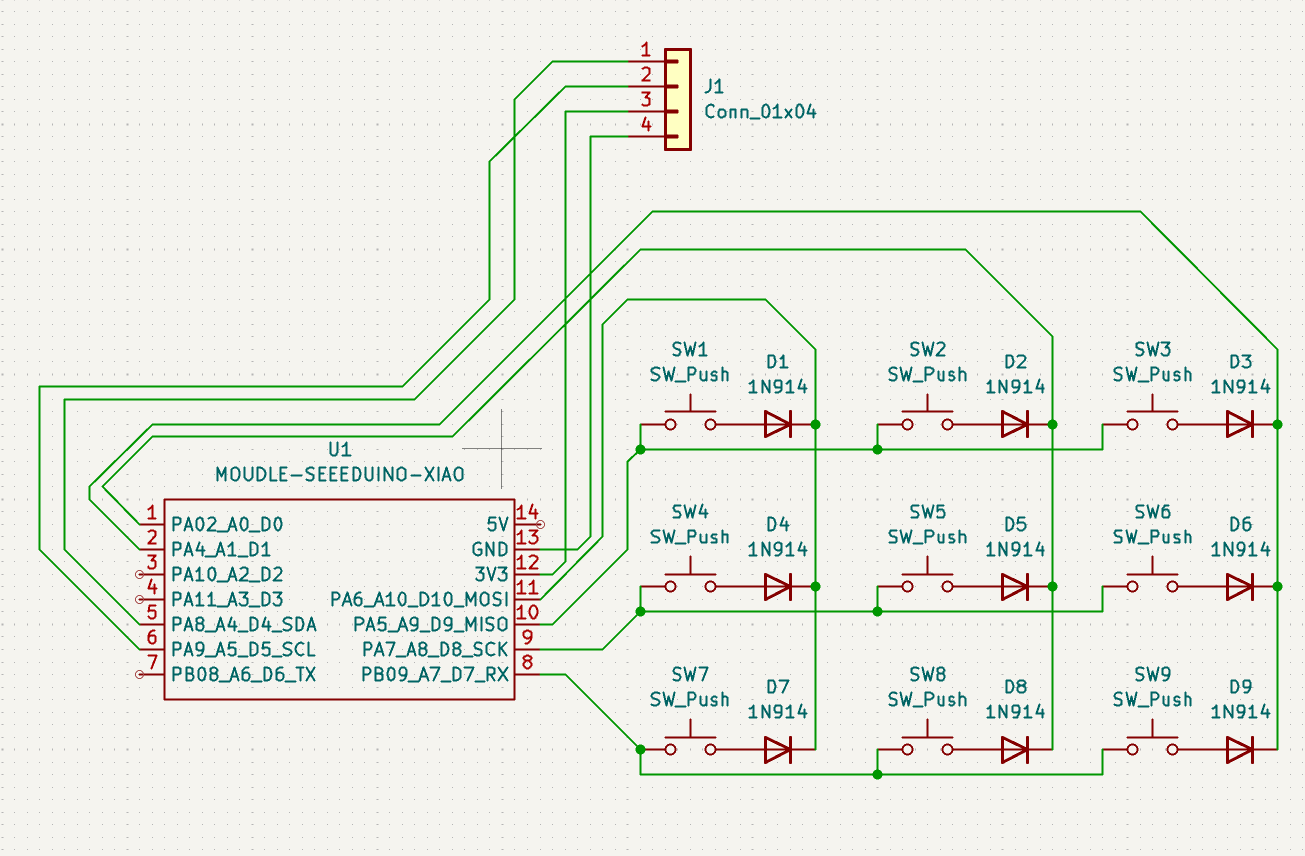
The controller is a Seeed Studio XIAO (SAMD21). The 9 switches form a 3×3 diode matrix and a 4-pin header standard 2.54 mm pitch, GND–VCC–SCL–SDA)
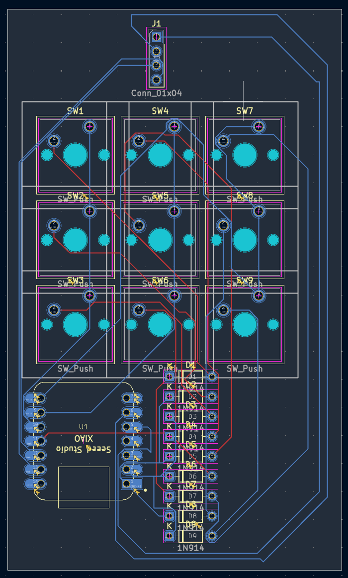
Designed in KiCad (see pcb/). Manufacturing files (gerbers) are in Production/gerbers.zip.
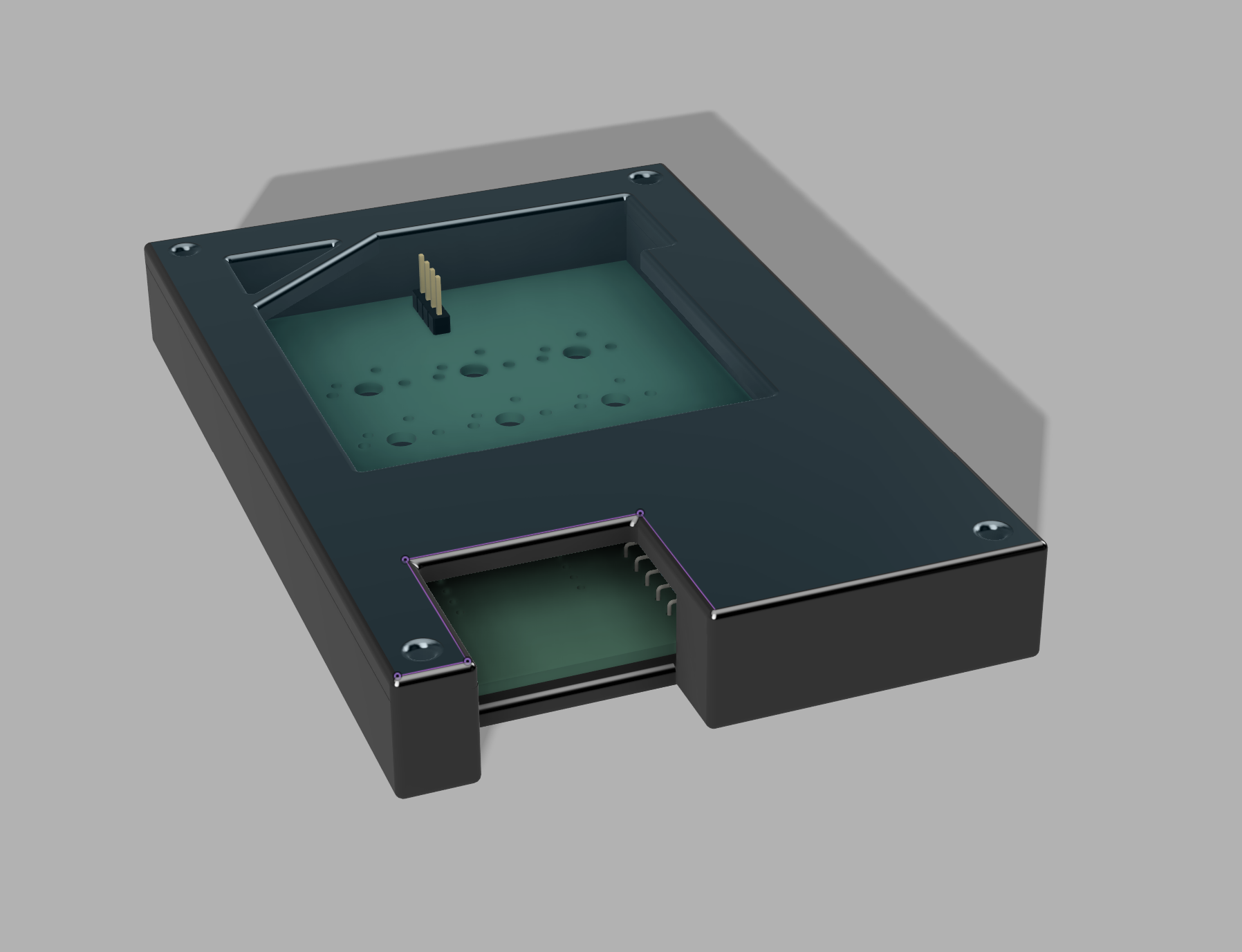
I modeled the case in Fusion 360. The case features a cutout for the XIAO's USB-C port and an opening for the 4-pin display header. You'll find the STEP files for the top and bottom shells in Production/, and the full assembly is in CAD/Assembly1.0.step.
| Part | Quantity |
|---|---|
| Seeed Studio XIAO | 1 |
| MX-style switches | 9 |
| 1N914 diodes | 9 |
| SSD1306 OLED display (128×32, I²C) | 1 |
| 4-pin header | 1 |
| M3 screws | 4 |
You can find the firmware in Firmware/or Production/Firmware.py and it is written for KMK, a CircuitPython-based keyboard firmware. code.py is the source; a compiled .hex build is included as well.
What it does:
board.D0–D2 (columns) and board.D7–D9 (rows), COL2ROW diode orientation7 8 9 / 4 5 6 / 1 2 3| Qty | Value | Footprint | References |
|---|---|---|---|
| 9 | 1N914 | Diode_THT:D_DO-35_SOD27_P7.62mm_Horizontal | D1, D2, D3, D4, D5, D6, D7, D8, D9 |
| 9 | SW_Push | Button_Switch_Keyboard:SW_Cherry_MX_1.00u_PCB | SW1, SW2, SW3, SW4, SW5, SW6, SW7, SW8, SW9 |
| 1 | Conn_01x04 | Connector_PinHeader_2.54mm:PinHeader_1x04_P2.54mm_Vertical | J1 |
| 1 | MOUDLE-SEEEDUINO-XIAO | footprints:XIAO-Generic-Hybrid-14P-2.54-21X17.8MM | U1 |
It measures 59.5 × 100 mm and has 2 copper layers, 1.6 mm thick.
20 parts. The full list of its parts is on this page, with links to each part's symbol and footprint where PCBKit's library has them.
From the javinwittig/Hackpad repository on GitHub, at the commit this page was made from: the board is pcb/Schaltplatte_6_Tasten.kicad_pcb and its schematic pcb/Schaltplatte_6_Tasten.kicad_sch. PCBKit opens the board in the browser, with nothing to install.
Its repository states no licence, so its author keeps all rights: ask javinwittig before reusing the design.


atopile/atopile
Design circuit boards with code! ✨ Get software-like design reuse 🚀, validation, version control and collaboration in hardware; starting with electronics ⚡️

davidphilipbarr/Sweep
Sweep - a small promicro based keyboard inspired by the Ferris.

rusefi/rusefi
rusefi - GPL internal combustion engine control unit

hoglet67/RGBtoHDMI
Bare-metal Raspberry Pi project that provides pixel-perfect sampling of Retro Computer RGB/YUV video and conversion to HDMI

hackclub/OnBoard
💡 Join 1,000 teenagers and make your first PCB with a $100 grant!

FreeYourStream/freedeck-hardware
all the stuff you need to build your own FreeDeck