
4 layers99 × 53.3 mm
PSLab
fossasia/pslab-hardware
PSLab Hardware Design and Schematics https://pslab.io
199 parts1.7kApache-2.0

 jamallyemin/hackpad-macropad
very kewl 3-key macropad made for hack club hackpad!
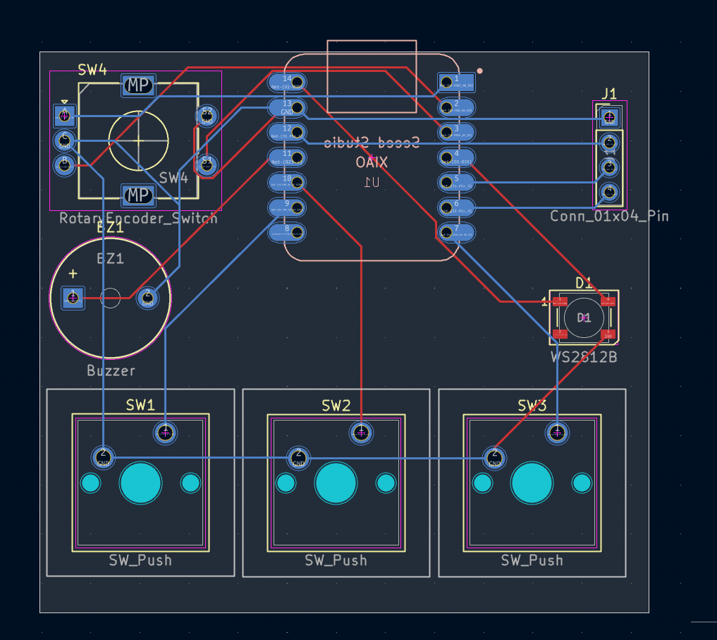
Hackpad is an open-source printed circuit board by jamallyemin, from the jamallyemin/hackpad-macropad repository on GitHub. It is a 2-layer board of 62 × 57 mm with 8 parts on 15 nets, routed with 67 tracks and 0 vias.
It is built around the WS2812B. Its parts include 4 switches, 1 IC, 1 diode and 1 connector.
very kewl 3-key macropad made for hack club hackpad!
it's a compact custom macropad featuring a rotary encoder, 0.91" OLED screen, WS2812B RGB LED, and a piezo buzzer for cool noises/audio feedback. everything is powered by the Seeed Studio XIAO RP2040 placed right at the top of the board!
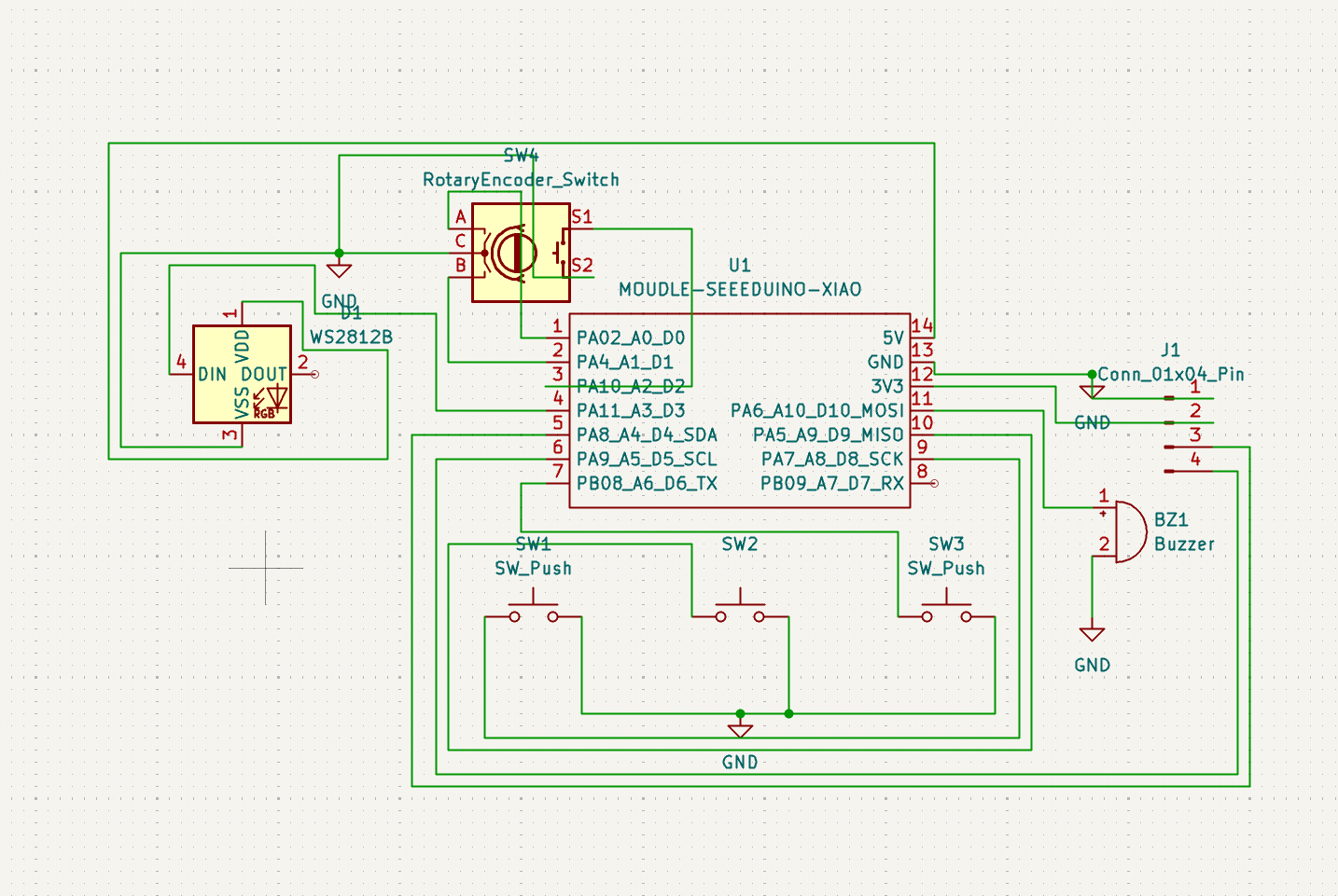
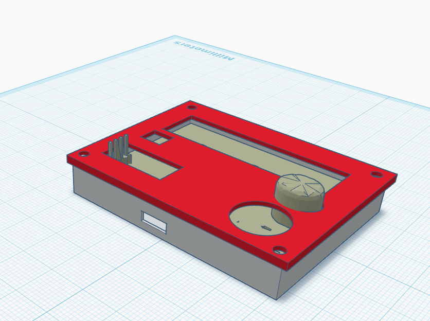
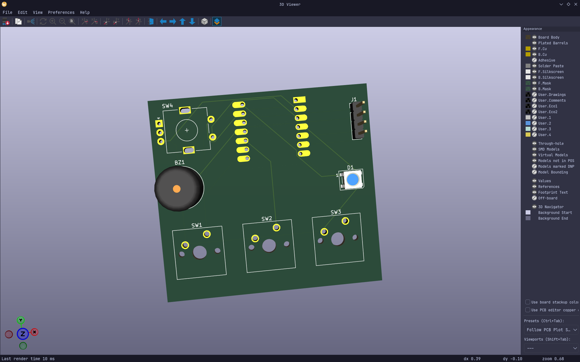
/PCB - KiCad schematic (.kicad_sch), PCB layout (.kicad_pcb), and project files./CAD - 3D model STEP files (hackpad.step)./production - Gerber files (gerbers.zip), 3D printable STL files (Top.stl, Bottom.stl), and production code./images - Screenshots and 3D preview renders./Firmware - CircuitPython code (main.py).The enclosure consists of 2 custom 3D printed parts: Top.stl and Bottom.stl. Everything fits together neatly to protect the PCB and hold the mechanical switches firmly in place. Designed in CAD and exported to /CAD/hackpad.step.
Designed using KiCad! The layout puts the XIAO RP2040 at the top edge of the board to allow seamless USB cable plugging without hitting the case walls. All footprints and traces are verified with zero DRC errors.
Runs using CircuitPython / MicroPython (main.py).
Here's everything needed to build this hackpad:
Top.stl)Bottom.stl)| Qty | Value | Footprint | References |
|---|---|---|---|
| 3 | SW_Push | Button_Switch_Keyboard:SW_Cherry_MX_1.00u_PCB | SW1, SW2, SW3 |
| 1 | Buzzer | Buzzer_Beeper:Buzzer_12x9.5RM7.6 | BZ1 |
| 1 | Conn_01x04_Pin | Connector_PinHeader_2.54mm:PinHeader_1x04_P2.54mm_Vertical | J1 |
| 1 | MOUDLE-SEEEDUINO-XIAO | footprints:XIAO-Generic-Hybrid-14P-2.54-21X17.8MM | U1 |
| 1 | RotaryEncoder_Switch | Rotary_Encoder:RotaryEncoder_Alps_EC11E-Switch_Vertical_H20mm | SW4 |
| 1 | WS2812B | LED_SMD:LED_WS2812B_PLCC4_5.0x5.0mm_P3.2mm | D1 |
It measures 62 × 57 mm and has 2 copper layers, 1.6 mm thick.
8 parts, built around the WS2812B. The full list of its parts is on this page, with links to each part's symbol and footprint where PCBKit's library has them.
From the jamallyemin/hackpad-macropad repository on GitHub, at the commit this page was made from: the board is PCB/hackpad.kicad_pcb and its schematic PCB/hackpad.kicad_sch. PCBKit opens the board in the browser, with nothing to install.
Its repository states no licence, so its author keeps all rights: ask jamallyemin before reusing the design.
fossasia/pslab-hardware
PSLab Hardware Design and Schematics https://pslab.io

FrameworkComputer/ExpansionCards
Reference designs and documentation to create Expansion Cards for the Framework Laptop


PrintersForAnts/Micron
If you want to purchase full kits there are 3 available (Kits are slowly updating to R1 hardware just make sure to double check the included hardware in your kit and if you have any questions reach out in the discord)


