
4 layers80 × 60 mm
Tinynode
Stary2001/my-mesh-nodes
Here's all my mesh stuff. Everything here is licensed under CERN OHL-P.
67 parts2CERN-OHL-P-2.0

 jaisor/SolarMeshMiniPDB
20 x 12 mm solar charger (CN3163) and power distribution board for a mini handheld LoRa mesh node. KiCad 10.
SolarMeshMiniPDB is an open-source printed circuit board by jaisor, from the jaisor/SolarMeshMiniPDB repository on GitHub. It is a 2-layer board of 20 × 12 mm with 14 parts on 9 nets, routed with 31 tracks and 17 vias.
It is built around the CN3163. Its parts include 4 connectors, 3 resistors, 2 capacitors, 2 diodes and 1 IC. It belongs with the power and radio and wireless boards of this library.
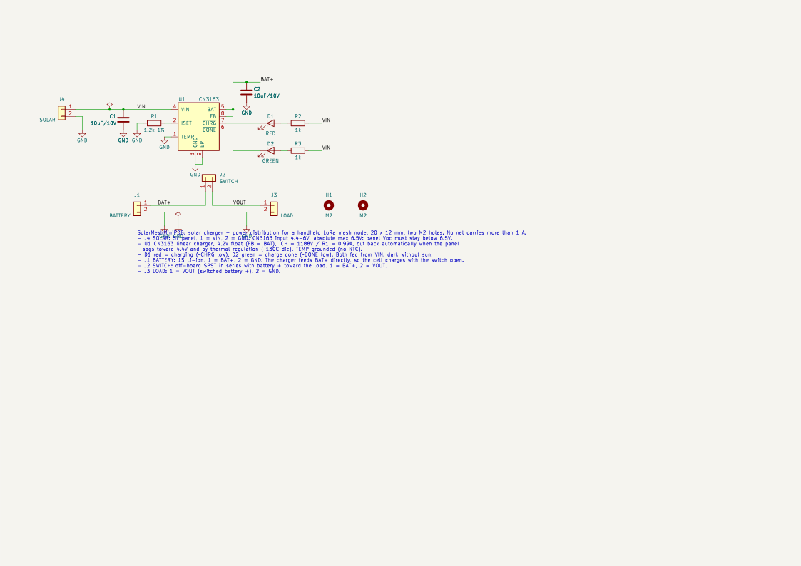
Minimal solar charger and power distribution board, sized to power a mini handheld LoRa mesh node. It has solder pads for a 5 V solar panel, a 1S Li-ion battery, a load, and an external switch that breaks the positive wire to the load. A CN3163 charges the battery from the panel at up to 1 A, like the SD05CRMA module, with the same two status LEDs: red while charging, green when the battery is full. 20 × 12 mm, two M2 mounting holes.
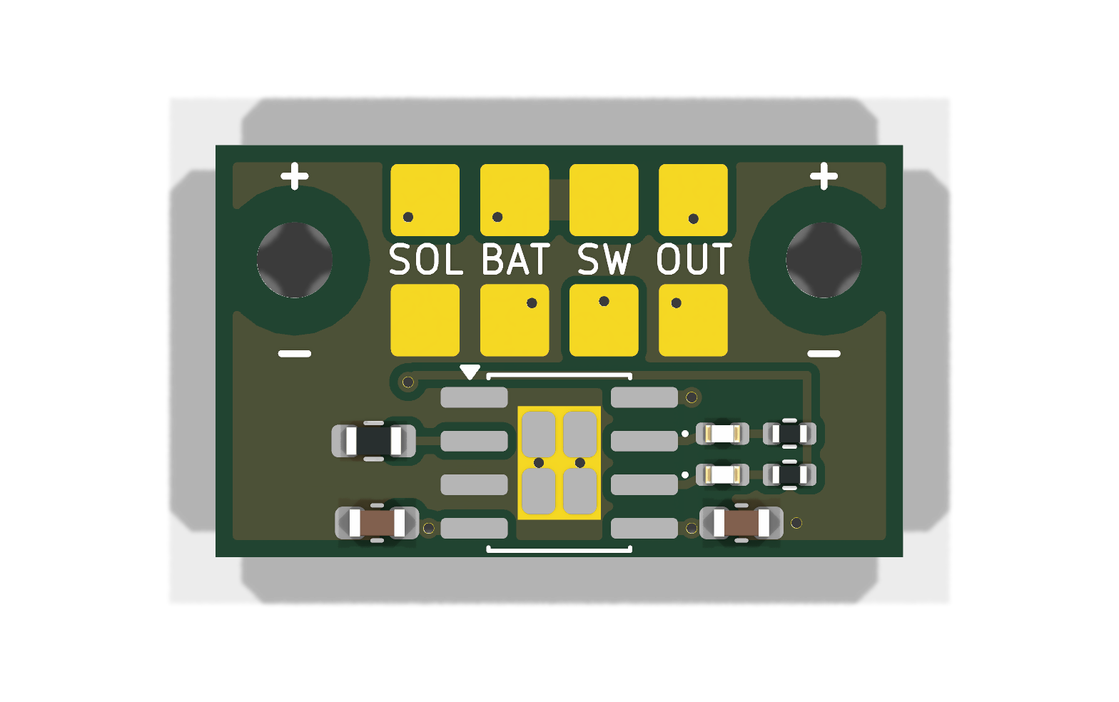
| Pads | Top (+) | Bottom (−) |
|---|---|---|
| SOL | solar panel + | solar panel − |
| BAT | battery + | battery − |
| SW | switch, battery side | switch, load side |
| OUT | load + (switched) | load − |
The charger feeds the battery directly, so the battery keeps charging with the switch off; the switch only cuts the load. The switch is non-polar, so its two wires can go on either SW pad. All the − pads are connected.
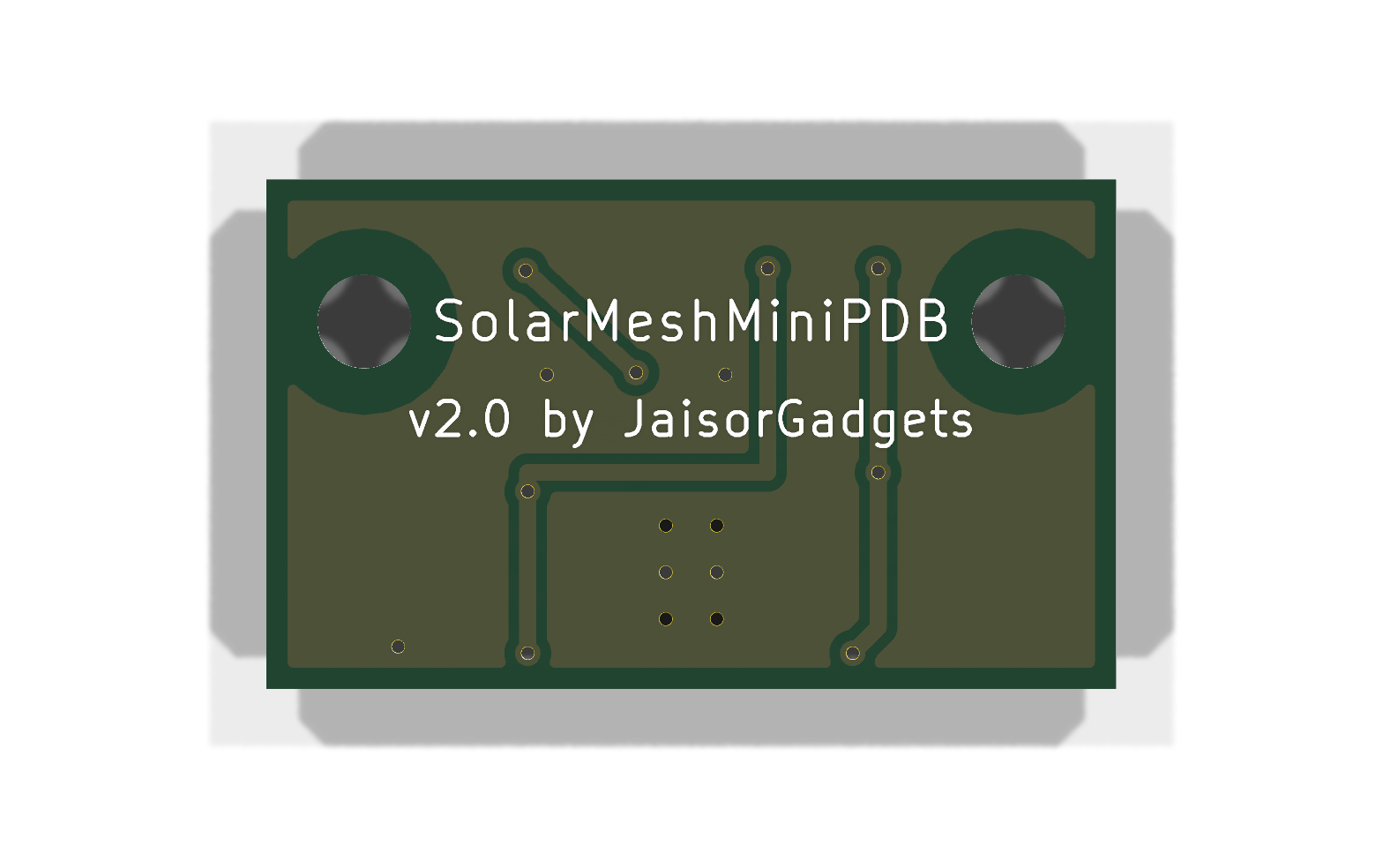
The back is a ground plane with three jumpers (solar input, battery, switched output) and six thermal vias under the CN3163.
The package is generated into output/fab/. It isn't tracked in git; regenerate it with the commands in CLAUDE.md.
| File | Contents |
|---|---|
SolarMeshMiniPDB_v2.0_gerbers.zip | Upload this to the board house: Gerbers incl. solder paste, drill files, job file. 2 layers, 1.6 mm, 1 oz copper |
SolarMeshMiniPDB_v2.0_BOM.csv | BOM in JLCPCB format with LCSC part numbers for every line |
SolarMeshMiniPDB_v2.0_CPL.csv | Pick-and-place file, top side only, same coordinates as the Gerbers |
FAB_NOTES.txt | Order settings and assembly cautions |
The CN3163 (C559031) and the two LEDs are JLCPCB Extended parts. Check the rotation of U1 and the LED polarity in the assembler's preview before ordering. The wire pads and mounting holes aren't parts, so they're not in the BOM or placement file.
The schematic and board are generated by the scripts in tools/; see CLAUDE.md for the commands.
| Qty | Value | Footprint | References |
|---|---|---|---|
| 2 | 10uF/10V | Capacitor_SMD:C_0603_1608Metric | C1, C2 |
| 2 | 1k | Resistor_SMD:R_0402_1005Metric | R2, R3 |
| 2 | M2 | MountingHole:MountingHole_2.2mm_M2 | H1, H2 |
| 1 | 1.2k 1% | Resistor_SMD:R_0603_1608Metric | R1 |
| 1 | BATTERY | SolarMeshMiniPDB:WirePad_1x02_SMD_2.0x2.1mm_P3.5mm | J1 |
| 1 | CN3163 | Package_SO:SOIC-8-1EP_3.9x4.9mm_P1.27mm_EP2.41x3.3mm | U1 |
| 1 | GREEN | LED_SMD:LED_0402_1005Metric | D2 |
| 1 | LOAD | SolarMeshMiniPDB:WirePad_1x02_SMD_2.0x2.1mm_P3.5mm | J3 |
| 1 | RED | LED_SMD:LED_0402_1005Metric | D1 |
| 1 | SOLAR | SolarMeshMiniPDB:WirePad_1x02_SMD_2.0x2.1mm_P3.5mm | J4 |
| 1 | SWITCH | SolarMeshMiniPDB:WirePad_1x02_SMD_2.0x2.1mm_P3.5mm | J2 |
It measures 20 × 12 mm and has 2 copper layers, 1.6 mm thick.
14 parts, built around the CN3163. The full list of its parts is on this page, with links to each part's symbol and footprint where PCBKit's library has them.
From the jaisor/SolarMeshMiniPDB repository on GitHub, at the commit this page was made from: the board is SolarMeshMiniPDB.kicad_pcb and its schematic SolarMeshMiniPDB.kicad_sch. PCBKit opens the board in the browser, with nothing to install.
Its repository states no licence, so its author keeps all rights: ask jaisor before reusing the design.
Stary2001/my-mesh-nodes
Here's all my mesh stuff. Everything here is licensed under CERN OHL-P.


LJBoxx/fantastic-node
meshtastic node designed to be solar powered and small enough to be planted in urban spaces.

google/mozc-devices
Circuit diagrams and firmware source code for Gboard DIY keyboards


hackclub/OnBoard
💡 Join 1,000 teenagers and make your first PCB with a $100 grant!

