

2 layers

This project is an implementation of an NFC tag which is able to change the message. It communicates to a host device.
Nfc tag is an open-source printed circuit board by Iceteavanill, from the Iceteavanill/NFC_message_switcher repository on GitHub. It is a 2-layer board of 85.6 × 54 mm with 17 parts on 11 nets, routed with 76 tracks and 2 vias.
It is built around the ATTINY402-SSN. Its parts include 3 capacitors, 2 resistors, 2 ICs and 1 connector. It belongs with the radio and wireless boards and the AVR (ATmega, ATtiny) boards of this library.
This project is an implementation of an NFC tag which is able to change the message. It communicates to a host device. It was developed to be quickly assembled and easy to use but still be a bit more than a blinking light. It uses the reference implementation for the bare metal TWI driver.
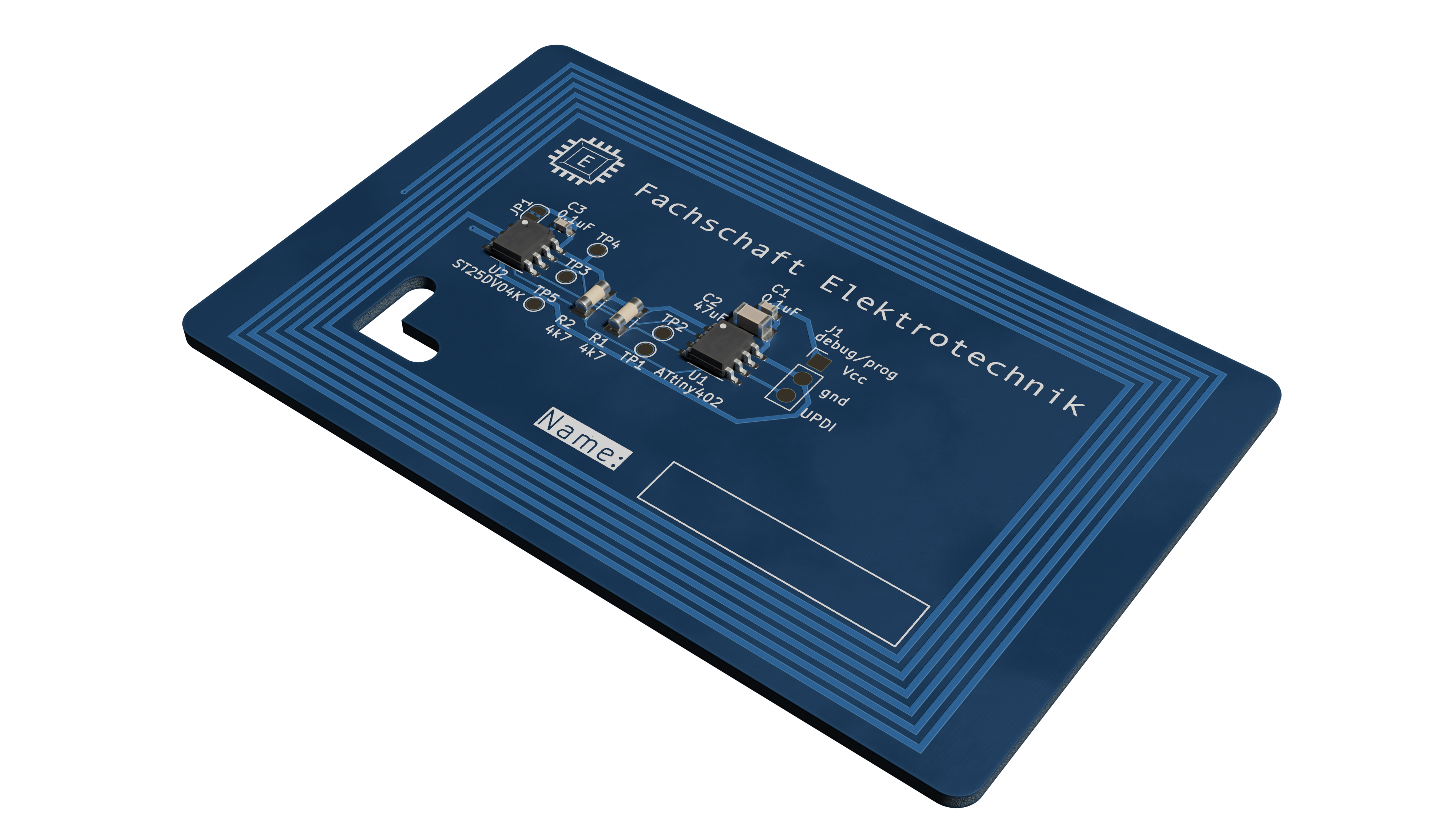
The main device is the ST25DV04K. It can communicate via NFC and I2C. When an NFC capable device is held near the PCB, the ST25DV04K starts to receive power and starts communicating with the device. The Power that's transmitted is shared (energy harvesting mode) with a ATtiny402. When powered it starts communicating via I2C and writes to the user accessible memory. When the written data has been confirmed, it powers down.
Power provider is the energy harvesting mode of the ST25DV04K, the power source is a NFC capable device that is in proximity of the PCB. It is buffered via a 47μF capacitor. Because of that, it is essential to keep the power consumption of the ATtiny as low as possible. Consult the source code for more details.
The ST25DV04K does only support I2C or NFC active at the same time. However, it has an open drain output that can be used to sense the current activity. Low, signals that the device is currently busy. The ATtiny then waits for the device to be available, by waiting in sleep. A hardware interrupt is not yet implemented.
The ST25DV04K needs some configuration for correct operation. The energy harvesting mode must be enabled/forced at startup. Also, the GPO mode must be set to RF_ACTIVITY_EN to enable better link arbitration. The configuration happens after the ATtiny has been programmed once.
The antenna / coil design is based on a paper from Hubert Aebischer. The ST25DV04K has an internal tuning capacitor which should be assumed to be 29pF. Based on that, the inductance should be 4.75μH.
The PCB dimensions are the same as a credit card. It is however quite a bit thicker.
All required files to recreate this project can be found here.
The following parts are needed to recreate this Project (as well as the PCB):
| Reference | Value | Qty | Digikey number |
|---|---|---|---|
| C1, C3 | 0.1uF | 2 | 1276-1000-1-ND |
| C2 | 47uF | 1 | 1276-3063-2-ND |
| R1, R2 | 4k7 | 2 | MMA-4.7KACT-ND |
| U1 | ATtiny402 | 1 | ATTINY402-SSNRCT-ND |
| U2 | ST25DV04K | 1 | 497-17123-1-ND |
There are no special requirements for the assembly of the PCB's. If you are used to soldering SMD components it shouldn0t be a problem.
You can use the provided released hex file, however it is recommended to customize the software to your own taste.
There are multiple options to customize the software
[!WARNING]
I tried making the process of using the software as easy as possible, however it may not be very easy/beginner-friendly in places.
Customizing the software always requires a rebuild of the firmware of the Attiny. The XC8 compiler from microchip is recommended. The following flags were used and are recommended:
| Flags | commands |
|---|---|
| Global | -gdwarf-3 -mconst-data-in-progmem -mno-const-data-in-config-mapped-progmem |
| compiler | -funsigned-char -funsigned-bitfields -Wall -O2 -fno-common |
| linker | "libm" -Wl,--gc-sections |
A makefile is already prepared with all the required flags. If you install a later version you might have to alter the paths a little.
For customization, only a header file has to be altered (nfc_messages.h).
There are multiple ways of accomplishing that:
Editing the header directly is not recommended because the required data must be in the NDEF format. Manually generating that is very tedious. If you have special needs however, like encoding special data types, you have to do it this way because anything else has not been implemented.
The dataGenerator.py python script can be used to quickly generate custom messages.
It requires the NDEFLib python library.
Edit the message_as_text_list list with your messages and then run the script:
message_as_text_list = ["Test 1",
                        "Test 2 a bit longer",
                        "Test 3 even looooooooooooooooooooooooooonger",
                        "https://www.youtube.com/watch?v=dQw4w9WgXcQ",
                        "spotify:track:4cOdK2wGLETKBW3PvgPWqT"
]A gui has been made to quickly program multiple NFC tags.
It requires WXpython and uses the previously mentioned script and the message_as_text_list.
For uploading, it relies on the MPLAB IPE programming software and its command line interface.
Programming steps:
Enter your desired message(s) in the table at the top. Links to websites videos or Spotify songs are also allowed.
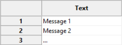
If your main device is an iPhone check the iPhone compatability mode.
IPhones are unable to read text from a NFC device, and the text messages have to be encoded as a website.
Some default messages are added to the list automatically. If you don't want that, you can disable that with the checkbox Remove predefined texts.
The message_as_text_list from dataGenerator.py is used as a source.
Connect your programmer to the tag and press program device. The build and upload steps are automatically executed.
In all options but the gui you have to manually build and then upload the firmware.
You can use the make upload command with the option PROGTOOL= to select the programmer that you have on hand.
See the documentation of the IPE programmer option to know which flag you have to use.
Many devices in a row can be programmed with the programming jig:
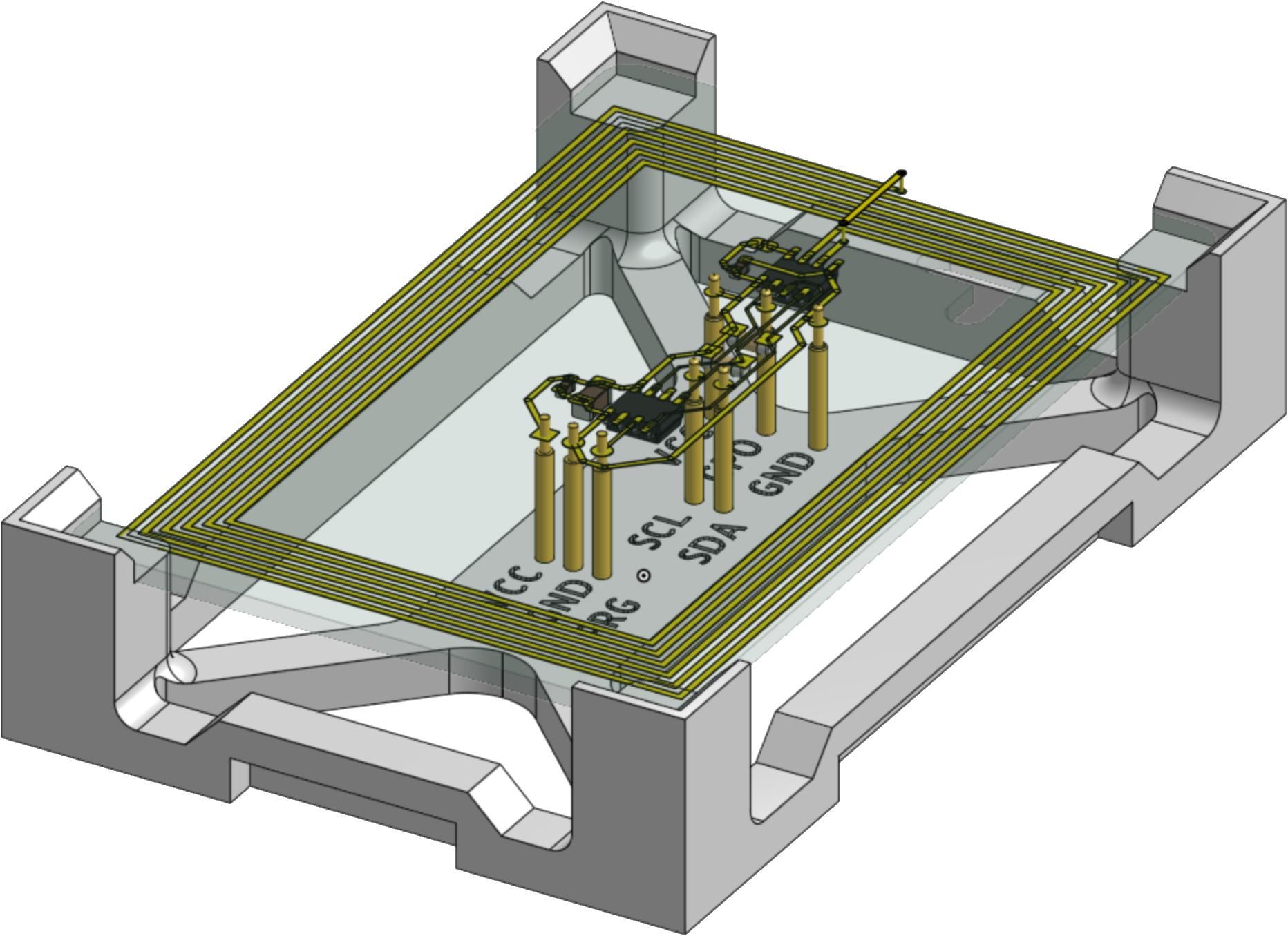
It was designed in Onshape. I used pogopins that I had on hand. You probably want to customize it to your current stock. You find the Onshape document here.
Because this PCB was designed as a competition PCB, a rating gui has been made using streamlit. You can import a CSV of contestants and rate each one for time, quality and some other points. It is meant to be customized to your particular use case.
It must be noted that the current design has a (obvious) flaw. The ATtiny is in the middle of the coil and probably quite affected by the activity of it. When combined with the nonideal power delivery method, this can significantly impair functionality at times (The I2C content that is written gets verified but I2C has no error correcting method). Some more analysis in that regard is not yet made.
| Qty | Value | Footprint | References |
|---|---|---|---|
| 2 | 0.1uF | Capacitor_SMD:C_0603_1608Metric_Pad1.08x0.95mm_HandSolder | C1, C3 |
| 2 | 4k7 | Resistor_SMD:R_MiniMELF_MMA-0204 | R1, R2 |
| 2 | LOGO | LOGO | G***, G*** |
| 1 | 47uF | Capacitor_SMD:C_1206_3216Metric_Pad1.33x1.80mm_HandSolder | C2 |
| 1 | ATtiny402 | Package_SO:SOIC-8_3.9x4.9mm_P1.27mm | U1 |
| 1 | Antenna_Loop | footprint_lib:nfc antenna_optimized | AE1 |
| 1 | NC | Jumper:SolderJumper-2_P1.3mm_Bridged2Bar_RoundedPad1.0x1.5mm | JP1 |
| 1 | ST25DV04K | Package_SO:SOIC-8-1EP_3.9x4.9mm_P1.27mm_EP2.29x3mm | U2 |
| 1 | Vcc | TestPoint:TestPoint_Pad_D1.5mm | TP4 |
| 1 | debug/prog | footprint_lib:debug_pads | J1 |
| 1 | gnd | TestPoint:TestPoint_Pad_D1.5mm | TP5 |
| 1 | gpo | TestPoint:TestPoint_Pad_D1.5mm | TP3 |
| 1 | scl | TestPoint:TestPoint_Pad_D1.5mm | TP1 |
| 1 | sda | TestPoint:TestPoint_Pad_D1.5mm | TP2 |

PocketConcepts/Pocket_PSU
A variable current & voltage PSU with 3S lipo charging, balancing, and protection circuit using PPS.

k-takata/PCB_avr_dx_unbricker
UPDI High Voltage programmer for AVR Dx/Ex series

HazeCore/Nametag_Hardware
This is the hardware for out Nametag Badge for Chaos Communication Camp 2023. You can find more information about the Project at https://hazeco.re/cccamp-nametag/.

markusgruen/DccFunctionDecoder
Open source, Arduino-based DCC function decoder


KNEAGHUST/PCB_Christmas_Tree_AGH
PCB Christmas tree designed for the AGH University of Krakow

It measures 85.6 × 54 mm and has 2 copper layers, 1.6 mm thick.
17 parts, built around the ATTINY402-SSN. The full list of its parts is on this page, with links to each part's symbol and footprint where PCBKit's library has them.
From the Iceteavanill/NFC_message_switcher repository on GitHub, at the commit this page was made from: the board is hardware/pcb/nfc_tag.kicad_pcb and its schematic hardware/pcb/nfc_tag.kicad_sch. PCBKit opens the board in the browser, with nothing to install.
Its repository states no licence, so its author keeps all rights: ask Iceteavanill before reusing the design.