
2 layers49 × 32.1 mm
Pocket cape
hzeller/ldgraphy
Simple Laser Direct Lithography / Laser Direct Imaging for PCB manufacturing
29 parts321GPL-3.0

 hzeller/ldgraphy321
Simple Laser Direct Lithography / Laser Direct Imaging for PCB manufacturing
Laser drive is an open-source printed circuit board by hzeller, from the hzeller/ldgraphy repository on GitHub, published under the GPL-3.0 licence. It is a 2-layer board of 28.6 × 32.4 mm with 29 parts on 12 nets, routed with 166 tracks and 1 via.
It is built around the BCP5616QTA. Its parts include 11 capacitors, 7 resistors, 2 transistors, 2 connectors and 1 IC.
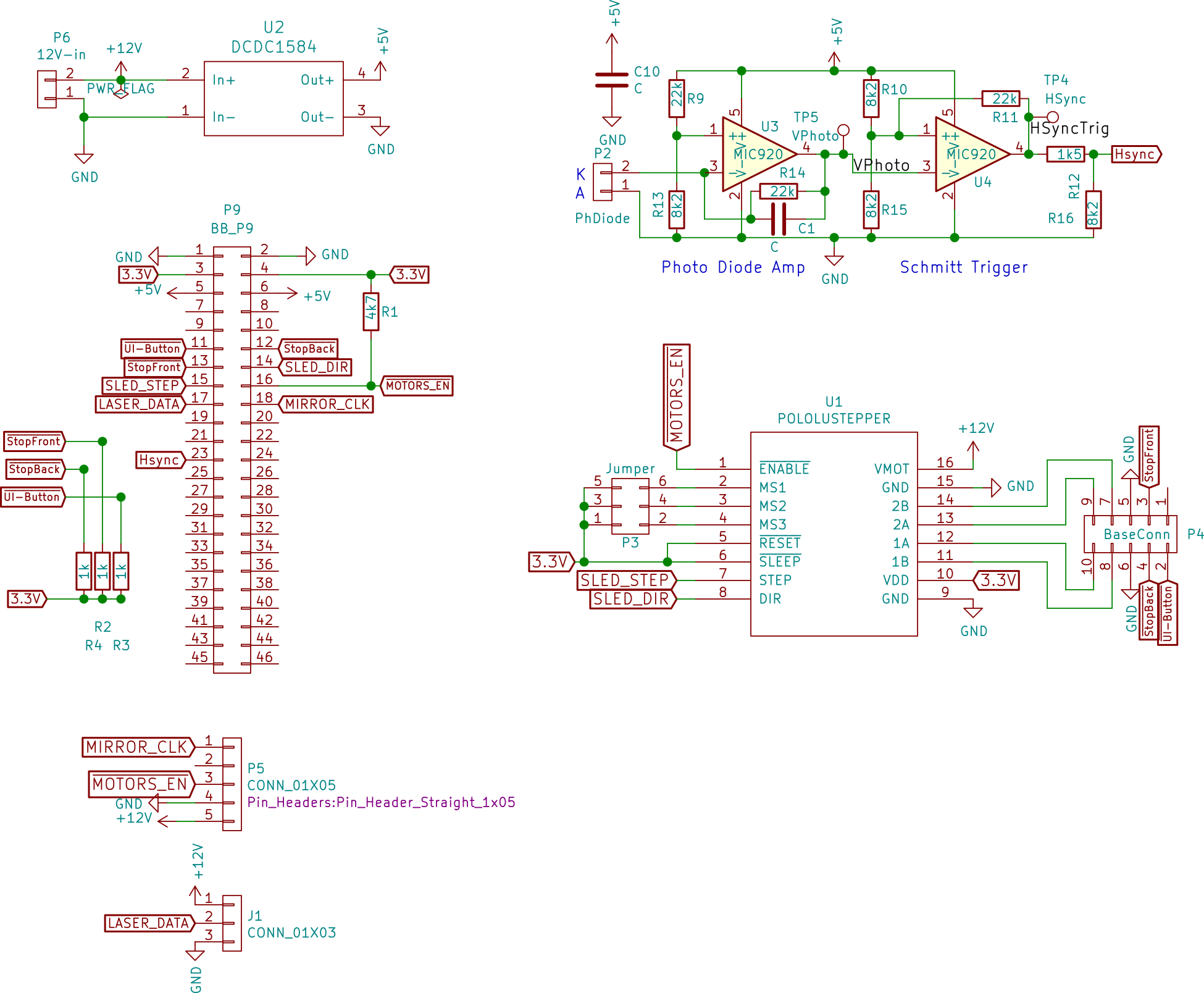
This is for the experimental set-up. This is not meant to be final, it focuses on easy measurement and mostly being a break-out for connectors for other parts. The final board will have all the parts that are now external modules integrated on one board.
(TODO: update schematic: there is now a cap accross R14)
| Qty | Value | Footprint | References |
|---|---|---|---|
| 7 | 10u | Capacitor_SMD:C_1210_3225Metric | C2, C3, C4, C5, C6, C7, C8 |
| 3 | 6R2 | Resistor_SMD:R_2512_6332Metric | R1, R5, R7 |
| 2 | 100n | Capacitor_SMD:C_0603_1608Metric | C1, C11 |
| 1 | 100n | Capacitor_SMD:C_0805_2012Metric | C9 |
| 1 | 100p | Capacitor_SMD:C_0603_1608Metric | C10 |
| 1 | 10k | Potentiometer_THT:Potentiometer_Bourns_3296X_Horizontal | RV1 |
| 1 | 1k | Resistor_SMD:R_0603_1608Metric | R8 |
| 1 | 2k2 | Resistor_SMD:R_0603_1608Metric | R2 |
| 1 | 470 | Resistor_SMD:R_0603_1608Metric | R3 |
| 1 | 5V6 | Diode_SMD:D_SOD-323_HandSoldering | D1 |
| 1 | 680 | Resistor_SMD:R_0603_1608Metric | R6 |
| 1 | BCP5616Q | Package_TO_SOT_SMD:SOT-223-3_TabPin2 | Q1 |
| 1 | CONN_01X03 | Connector_JST:JST_EH_B3B-EH-A_1x03_P2.50mm_Vertical | J1 |
| 1 | Control-Out | TestPoint:TestPoint_Pad_D1.5mm | TP3 |
| 1 | Current | TestPoint:TestPoint_Pad_D1.5mm | TP4 |
| 1 | LaserOut | Connector_JST:JST_EH_B2B-EH-A_1x02_P2.50mm_Vertical | P1 |
| 1 | MIC920 | Package_TO_SOT_SMD:SOT-353_SC-70-5 | U2 |
| 1 | MTM232270 | Package_TO_SOT_SMD:SOT-323_SC-70 | Q2 |
| 1 | VRef | TestPoint:TestPoint_Pad_D1.5mm | TP1 |
| 1 | VSense | TestPoint:TestPoint_Pad_D1.5mm | TP2 |
hzeller/ldgraphy
Simple Laser Direct Lithography / Laser Direct Imaging for PCB manufacturing

hzeller/ldgraphy
Simple Laser Direct Lithography / Laser Direct Imaging for PCB manufacturing

Secoh/Electronics
Educational etudes related to electronics, schematics, PCB layout, etc.

gusmanb/logicanalyzer
24 channel, 100Msps logic analyzer hardware and software

VoronDesign/Voron-Hardware
Cool Hardware designed by the Voron Design group

hoglet67/RGBtoHDMI
Bare-metal Raspberry Pi project that provides pixel-perfect sampling of Retro Computer RGB/YUV video and conversion to HDMI

hackclub/OnBoard
💡 Join 1,000 teenagers and make your first PCB with a $100 grant!

OLIMEX/DIY-LAPTOP
Do It Yourself Open Source Hardware and Software Modular Hacker's Friendly Laptop

UtilitechAS/amsreader-firmware
ESP8266 and ESP32 compatible firmware to read, interpret and publish data to MQTT from smart electrical meters, both DLMS and DSMR is supported

It measures 28.6 × 32.4 mm and has 2 copper layers, 1.6 mm thick.
29 parts, built around the BCP5616QTA. The full list of its parts is on this page, with links to each part's symbol and footprint where PCBKit's library has them.
From the hzeller/ldgraphy repository on GitHub, at the commit this page was made from: the board is pcb/laser-drive/laser-drive.kicad_pcb and its schematic pcb/laser-drive/laser-drive.kicad_sch. PCBKit opens the board in the browser, with nothing to install.
Its repository publishes it under the GPL-3.0 licence: you may reuse it on that licence's terms (keep the author's notice, and for a copyleft licence share your changes alike).