
2 layers251 × 148.4 mm
 huzi-ctrl/split-keyboard
Both the left and right halves share a modular hierarchical schematic (side.kicadsch):
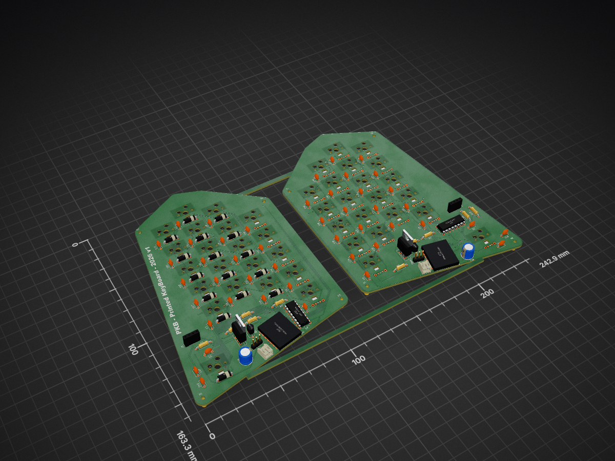
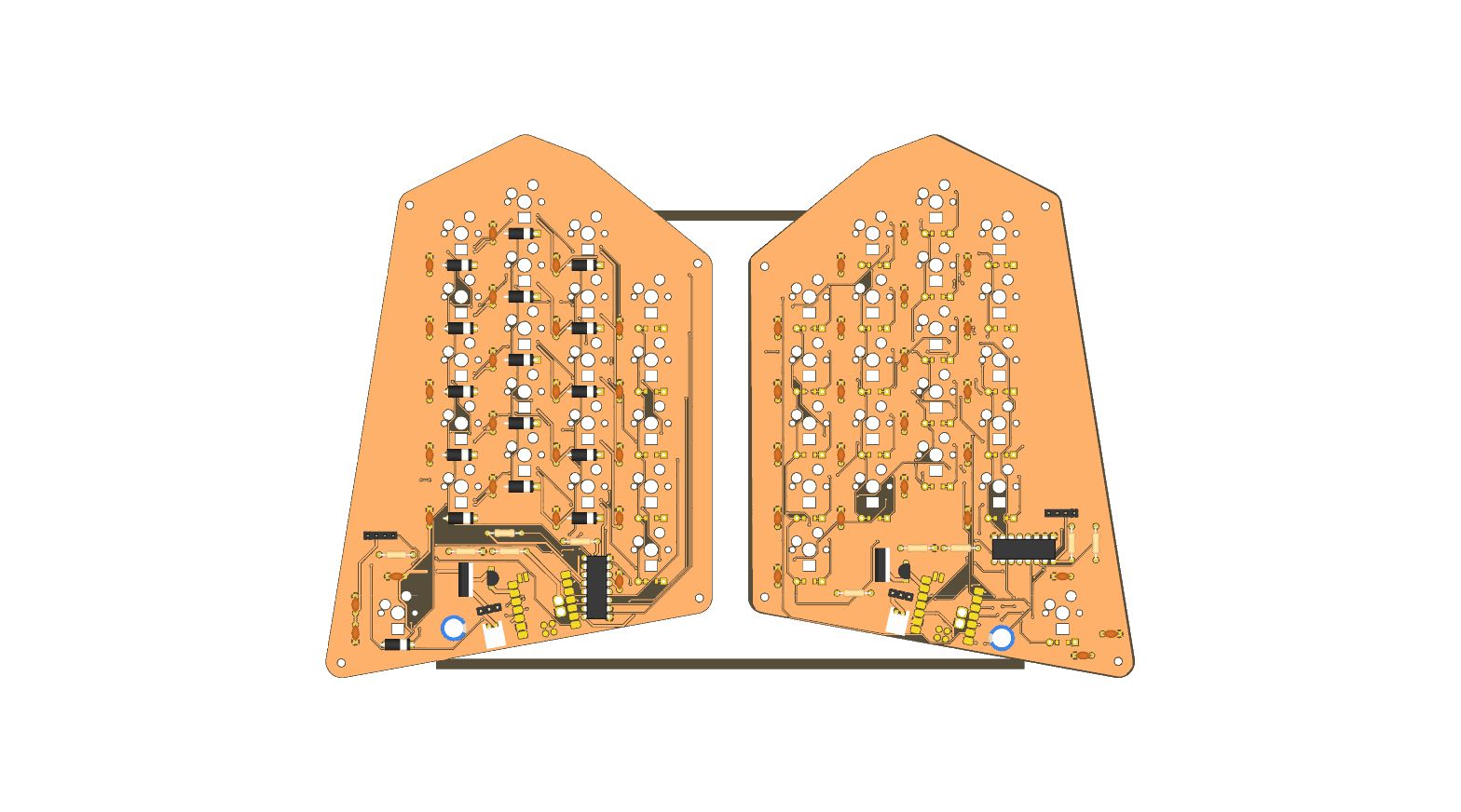
Keyboard is an open-source printed circuit board by huzi-ctrl, from the huzi-ctrl/split-keyboard repository on GitHub. It is a 2-layer board of 242.8 × 163.2 mm with 206 parts on 150 nets, routed with 1,926 tracks and 238 vias.
It is built around the PCF8574AP and SK6812MINI-E. Its parts include 84 diodes, 48 capacitors, 44 switches, 10 resistors and 4 ICs. It belongs with the keyboards and input boards and the nRF52 and nRF5x boards of this library.


PKB (Printed KeyBoard) is a custom 42-key wireless split mechanical keyboard designed from scratch in KiCad 10 and SolidWorks, powered by dual Seeed Studio XIAO nRF52840 microcontrollers running ZMK Firmware.
Traditional keyboards force your wrists to angle inward and make your fingers stretch across 6+ rows to reach numbers, symbols, and navigation keys. I wanted to design a compact, fully wireless split keyboard where:
BO1–BO3) to make fabrication and assembly clean and cost-effective.Seeed Studio XIAO nRF52840): Each half runs a XIAO nRF52840 (U1/U2). The left half acts as the central controller (connecting to up to 4 devices over Bluetooth Low Energy or USB-C), while the right half pairs wirelessly over BLE to the left half.PCF8574AP): Because the XIAO nRF52840 has only 11 GPIO pins, the 5 matrix columns (COL0–COL4) are driven directly by the XIAO (D1–D5), while the 5 matrix rows (ROW0–ROW4) are read through an NXP PCF8574AP 8-bit I2C I/O expander (U3/U4) on a shared I2C bus (SCL on D9, SDA on D10).J3/J4): Each half includes an I2C SSD1306 128×32 OLED display showing live battery percentage (%), active layer name (QWERTY, CODE / NAV, NUM / FN), and USB/Bluetooth profile status, with automatic 30-second idle blanking.42× SK6812MINI) with High-Side MOSFET Power Cut (Q1–Q4): Each half features 21 addressable SK6812MINI LEDs driven by hardware SPI (D0) and powered from VBAT through an NMOS+PMOS (Q1/Q3, Q2/Q4) high-side load switch (D8) so LED quiescent draw can be completely cut off to preserve battery life.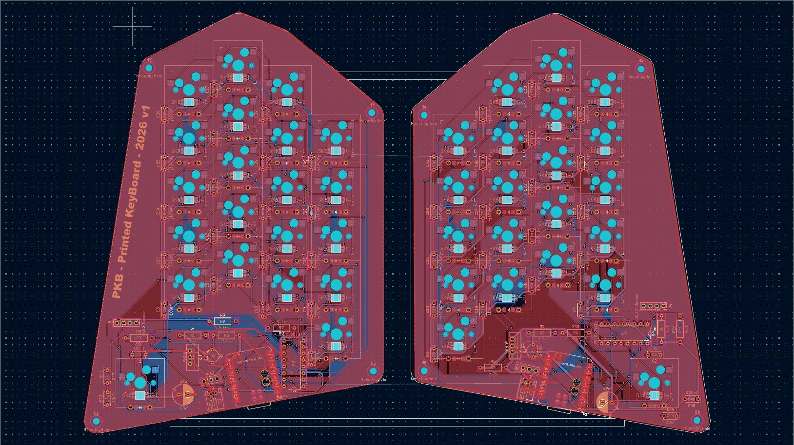
Both the left and right halves share a modular hierarchical schematic (side.kicad_sch):
/left/)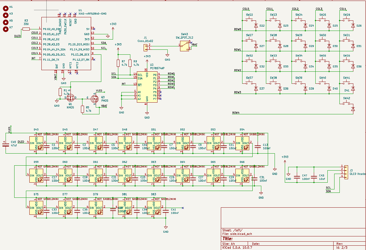
/right/)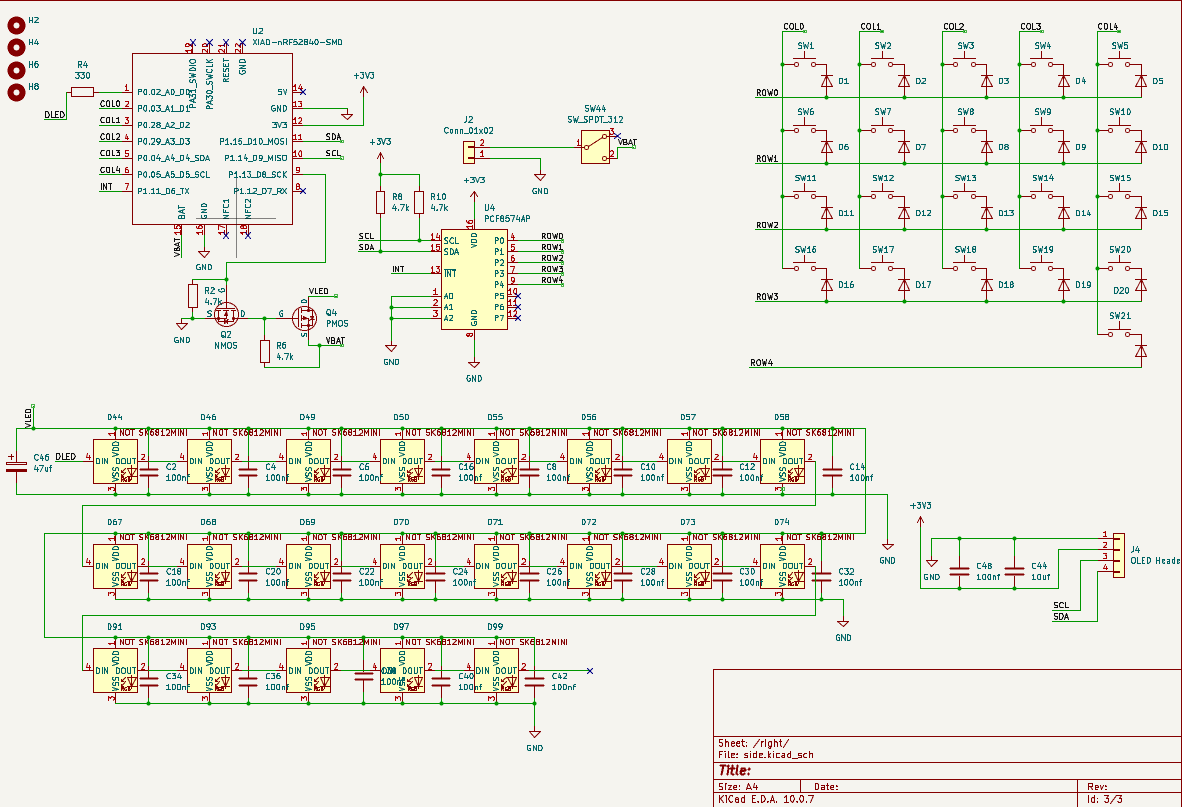
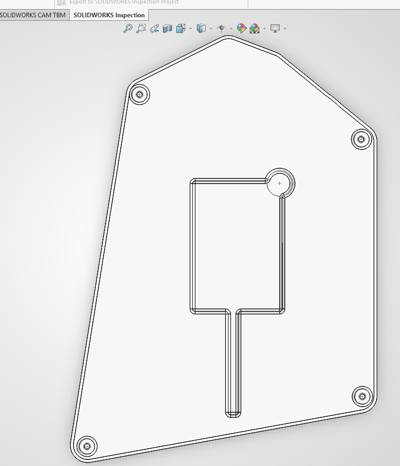
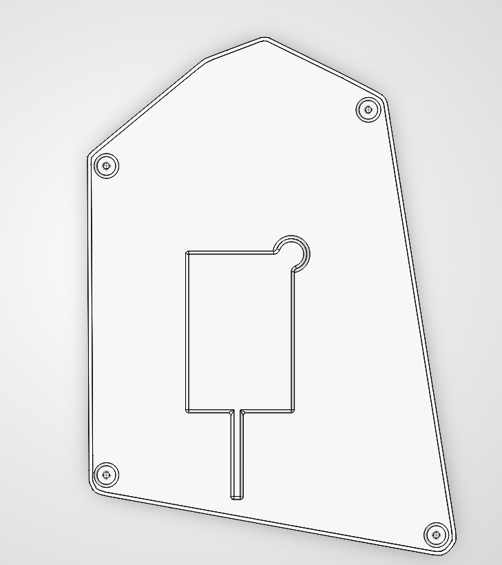
Custom 3D-printed enclosures modeled in SolidWorks with integrated battery compartment and cable routing channel (available in .STEP, .SLDPRT, and .3MF formats inside CAD/):
Left Half Enclosure (left_cad.png) | Right Half Enclosure (right_cad.png) |
|---|---|
 |  |
| Function | XIAO nRF52840 Pin | Peripheral / Notes |
|---|---|---|
DLED (RGB Data) | D0 (P0.02) | 21× SK6812MINI addressable RGB LEDs per half (&spi2 MOSI via 330 $\Omega$ resistor) |
COL0 – COL4 | D1 – D5 (P0.03, P0.28, P0.29, P0.04, P0.05) | Matrix column outputs (GPIO_ACTIVE_LOW, col2row) |
INT (Expander Interrupt) | D6 (P1.11) | Connected to PCF8574AP /INT (Pin 13) |
VLED Power Switch | D8 (P1.13) | Drives NMOS $\rightarrow$ PMOS high-side switch for VLED (ext-power) |
SCL (I2C Clock) | D9 (P1.14) | i2c0 (&xiao_i2c) with 4.7 k$\Omega$ pull-up to +3V3 |
SDA (I2C Data) | D10 (P1.15) | i2c0 (&xiao_i2c) with 4.7 k$\Omega$ pull-up to +3V3 |
ROW0 – ROW4 | PCF8574AP P0 – P4 | I2C I/O Expander at address 0x38 (A0=A1=A2=GND) |
OLED Display (J3/J4) | I2C (SCL/SDA) | 128×32 SSD1306 OLED at address 0x3C |
ZMK)Pre-built .uf2 firmware binaries are automatically compiled by GitHub Actions and published to GitHub Releases:
pkb_left-seeeduino_xiao_ble-zmk.uf2pkb_right-seeeduino_xiao_ble-zmk.uf21 Tap = Space | 2 Taps = Toggle Layer 1 (CODE / NAV)1 Tap = Backspace | 2 Taps = Toggle Layer 2 (NUM / FN)QWERTY (Base)+-----------------------------------------+ +-----------------------------------------+
| Q | W | E | R | T | | Y | U | I | O | P |
| A | S | D | F | G | | H | J | K | L | ; |
| Z | X | C | V | B | | N | M | , | . | / |
| LCTRL | LSHFT | LALT | LGUI | ESC | | RGUI | RALT | RSHFT | RCTRL | ENTER |
+-------------------------------+---------+ +---------+-------------------------------+
| SPC/NAV | | BSP/NUM |
+---------+ +---------+CODE / NAV (Double-Tap Left Thumb)+-----------------------------------------+ +-----------------------------------------+
| ` | [ | ] | - | = | | PG_UP | HOME | UP | END | DEL |
| ~ | { | } | _ | + | | PG_DN | LEFT | DOWN | RIGHT | --- |
| --- | \ | | | < | > | | --- | --- | --- | --- | --- |
| --- | --- | --- | --- | --- | | --- | --- | --- | --- | --- |
+-------------------------------+---------+ +---------+-------------------------------+
| SPC/NAV | | --- |
+---------+ +---------+NUM / FN (Double-Tap Right Thumb)+-----------------------------------------+ +-----------------------------------------+
| F1 | F2 | F3 | F4 | F5 | | / | 7 | 8 | 9 | - |
| F6 | F7 | F8 | F9 | F10 | | * | 4 | 5 | 6 | + |
| F11 | F12 |RGB_TOG|EP_TOG |OUT_TOG | | 0 | 1 | 2 | 3 | . |
| BT 1 | BT 2 | BT 3 | BT 4 | BT_CLR | | --- | --- | --- | --- | --- |
+-------------------------------+---------+ +---------+-------------------------------+
| --- | | BSP/NUM |
+---------+ +---------+BO1, BO2, BO3) along the center spine.D63–D104)B.Cu) layer.Pin 3 = GND) of each SK6812MINI-E with the silkscreen marker on the PCB.D1–D42) & SMD MOSFETs (Q1–Q4)D1–D42): The ComboDiode footprints support either 1N4148W (SOD-123 SMD) diodes on F.Cu or B.Cu, or 1N4148 (DO-35 through-hole) diodes. Orient every diode's cathode band (|◁) toward the square pad (K).Q1–Q4): Solder the SOT-23 NMOS (Q1, Q2) and PMOS (Q3, Q4) transistors onto their designated SMD pads near the microcontroller area on each half.U3, U4)C1–C42) next to each RGB LED, plus the 100 µF bulk radial capacitors (C43, C44) across the VLED power rails.R1–R6): I2C SDA/SCL pull-ups and /INT pull-ups.R7, R8) & $100\text{ k}\Omega$ (R9, R10): MOSFET gate bias/pull-down resistors.R11, R12): RGB DIN data-line series resistors.U3, U4)—or DIP-16 IC sockets—ensuring the Pin 1 half-moon notch matches the PCB silkscreen.SW1–SW42): On the bottom (B.Cu) side of the PCB, solder all 42 Kailh Choc/MX hot-swap sockets onto their wide SMD pads, making sure they sit flat against the board and do not obstruct the switch center hole.U1, U2):
+ and - pads on the underside of the XIAO nRF52840 and route them to the PCB's battery input pads (J1/J2) and slide power switch (SW43/SW44).J3, J4): Solder the 4-pin OLED header (GND, VCC, SCL, SDA) so the OLED sits above the XIAO footprint.SW43, SW44) & LiPo Battery (J1, J2): Solder the 3-pin slide switch and the 2-pin JST-PH 2.0 mm battery connector..uf2 files from GitHub Releases:
pkb_left-seeeduino_xiao_ble-zmk.uf2pkb_right-seeeduino_xiao_ble-zmk.uf2XIAO-SENSE.pkb_left-seeeduino_xiao_ble-zmk.uf2 onto the drive. Repeat with pkb_right-seeeduino_xiao_ble-zmk.uf2 on the Right XIAO nRF52840.PKB via Bluetooth!CAD/3mf/left.3MF and CAD/3mf/right.3MF in PLA or PETG (0.2 mm layer height, 15–20% infill).J1/J2).├── CAD/
│ ├── Keyboard.step # Full 3D assembly in STEP format
│ ├── 3mf/ # Printable 3MF files (left.3MF, right.3MF)
│ └── Raw/ # Native SolidWorks part files (left.SLDPRT, right.SLDPRT)
├── kicad/
│ ├── Keyboard.kicad_pro # KiCad 10 project file
│ ├── Keyboard.kicad_sch # Top-level schematic sheet
│ ├── side.kicad_sch # Left/Right modular keyboard half schematic
│ └── Keyboard.kicad_pcb # Panelized 2-layer PCB layout
├── firmware/
│ ├── boards/shields/pkb/ # ZMK shield definition, devicetree, Kconfig, and C init
│ ├── config/ # Keymap and ZMK configuration
│ └── build.yaml # GitHub Actions build matrix
├── images/ # PCB, schematic, and CAD screenshots
└── production.zip # Ready-to-manufacture Gerber, Drill, and CPL files| Qty | Value | Footprint | References |
|---|---|---|---|
| 44 | 100nf | Capacitor_THT:C_Disc_D5.0mm_W2.5mm_P5.00mm | C1, C2, C10, C11, C12, C13, C14, C15, C16, C17, C18, C19, C20, C21, C22, C23 +28 |
| 42 | D | ComboDiode | D1, D2, D10, D11, D12, D13, D14, D15, D16, D17, D18, D19, D20, D21, D22, D23 +26 |
| 42 | SK6812MINI-E | ceoloide:led_SK6812mini-e (per-keysingle-side) | D43, D44, D45, D46, D47, D48, D49, D50, D51, D52, D53, D54, D55, D56, D57, D58 +26 |
| 42 | SW_Push | MX | SW1, SW2, SW10, SW11, SW12, SW13, SW14, SW15, SW16, SW17, SW18, SW19, SW20, SW21, SW22, SW23 +26 |
| 8 | 4.7k | Resistor_THT:R_Axial_DIN0207_L6.3mm_D2.5mm_P10.16mm_Horizontal | R1, R2, R5, R6, R7, R8, R9, R10 |
| 8 | MountingHole | MountingHole:MountingHole_2.2mm_M2 | H1, H2, H3, H4, H5, H6, H7, H8 |
| 2 | 10uf | Capacitor_THT:C_Disc_D5.0mm_W2.5mm_P5.00mm | C43, C44 |
| 2 | 330 | Resistor_THT:R_Axial_DIN0207_L6.3mm_D2.5mm_P10.16mm_Horizontal | R3, R4 |
| 2 | 47uf | Capacitor_THT:CP_Radial_D8.0mm_P3.50mm | C45, C46 |
| 2 | Conn_01x02 | Connector_JST:JST_PH_S2B-PH-K_1x02_P2.00mm_Horizontal | J1, J2 |
| 2 | NMOS | Package_TO_SOT_THT:TO-92-2_Wide | Q1, Q2 |
| 2 | OLED Header | Connector_PinSocket_2.54mm:PinSocket_1x04_P2.54mm_Vertical | J3, J4 |
| 2 | PCF8574AP | Package_DIP:DIP-16_W7.62mm | U3, U4 |
| 2 | PMOS | Package_TO_SOT_THT:TO-220-3_Vertical | Q3, Q4 |
| 2 | SW_SPDT_312 | Connector_PinHeader_2.54mm:PinHeader_1x03_P2.54mm_Vertical | SW43, SW44 |
| 2 | XIAO-nRF52840-SMD | modified:modified-XIAO-nRF52840-SMD | U1, U2 |
It measures 242.8 × 163.2 mm and has 2 copper layers, 1.6 mm thick.
206 parts, built around the PCF8574AP and SK6812MINI-E. The full list of its parts is on this page, with links to each part's symbol and footprint where PCBKit's library has them.
From the huzi-ctrl/split-keyboard repository on GitHub, at the commit this page was made from: the board is kicad/Keyboard.kicad_pcb and its schematic kicad/Keyboard.kicad_sch. PCBKit opens the board in the browser, with nothing to install.
Its repository states no licence, so its author keeps all rights: ask huzi-ctrl before reusing the design.


AudioMorphology/Europi
Opensource sequencer software for Raspberry Pi equipped with Eurorack-compatible hardware

AaronC81/delta-pico
Powerful scientific calculator based on the Raspberry Pi Pico


cutec-chris/PiScope
Goto Telescope with Raspberry PI HQ Camera and exchangable Objective Holders for DSLR Objectives

kellerkindt/bluepill_sensor
Bluepill stm31f103 ethernet sensor extension board with SW written in Rust