Processor
Open Source Hardware Processor
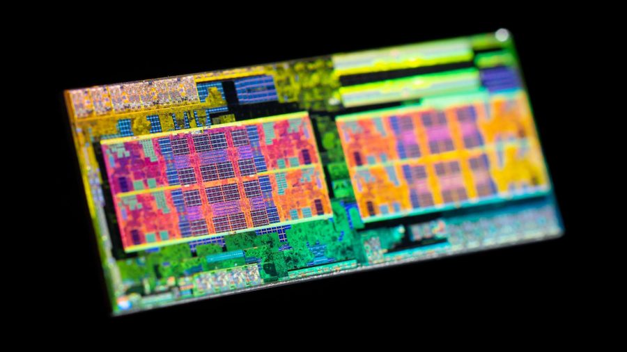
Mission
- Reduce the barrier to entry to open source silicon for hobbyists
- Encourage the production usage of fully open source, royalty-free, community designed ASICs within the maker community (displace proprietary chip designs)
- Shorten the iteration time from ideation to fabrication
- Explore creative ideas not found in current hardware offerings
- Interoperate with modern, high performance components that are typically the realm of proprietary designs (DDR4, PCIE root complex, USB3, etc come to mind)
- Make easy to use, relatively inexpensive hardware that people can acutally buy
Project Goals
Processor V1 (November 2020)
The software and the hardware parts can mostly be done simultaneously.
- Create a new CPU instruction set and design.
- it should be a sort of minimum viable 32 bit CPU. Something similar in capability to an Arduino, and with similar ports.
- Test the CPU design in simulators and on FPGA
- Fabricate the processor using Google and efabless free shuttle service for open source using 130nm process, and open source PDK
- Submit a design for the November free shuttle run.
- Try not to go too crazy with transistor count. We want to not be dependent on free fabrication in the future.
- Build an assembler for the ISA
- Make an Arduino-like board for the processor, with similar capabilities and supporting software
- Write or port C toolchain. Some higher level languages would also be nice, such as JS/python.
- TCC may be a good compiler to retarget for C.
- Here is what would be needed to be done to retarget it.
- Port as much of libc as possible. Uclib-ng or newlib would be good options.
Task List for V1 by Early November 2020 (exact deadline date to be determined):
- Design FPGA carrier board PCB. Get it manufactured, into peoples hands.
- This board has this FPGA board on it, https://www.robotshop.com/en/devantech-icewerx-ice40-hx8k-fpga.html?utm_source=google&utm_medium=surfaces&utm_campaign=surfaces_across_google_usen&gclid=EAIaIQobChMI5cem_Lyv6wIV0yCtBh2KFQhIEAYYASABEgJyuvD_BwE
- The board has SRAM and Flash chips built in.
- The board has latch chips to function as IO expanders because the fabricated CPU will be pin-limited.
- The board should have its own clock IC.
- Design ISA
- Write assembler for the ISA
- Get Verilog simulator up and running and documented.
- Design CPU and peripherals in Verilog or Migen.
- Simulate CPU and periherals in software. Programs should be able to run and take input/output.
- Test CPU and peripherals on the FGPA carrier board. RAM and flash should work. We should be able to load an run real programs on the board
- Create task list to prepare the verilog design for fabrication.
- Ensure we haven't overlooked anything that could cause our design to be rejected by Google/Skywater
- Ensure our design might actually work when fabricated
Fun Side Project for V1 : Make an Apple II or commodore style standalone PC using the processsor.
Processor V2 (Early 2021)
- Replicate V1 using non-donated fabrication and make the process economically sustainable.
- This means making chips and boards than people can actually buy.
- See Target Silicon section below.
- In theory, multi project wafer runs on very old tech could be < $100 per chip. Costs will go down as volume increases.
- we could do a Kickstarter or similar to fund a larger fabrication run for V2.
- Expand capabilities with software support
- more RAM, faster RAM
- graphics framebuffer
- more ports in general.
- Port other languages.
- MicroPython may be a good option.
- Build a LLVM backend.
- This is a lot of work, so it could be done in V2 or V3.
- A basic OS. This would be similar to old computers running BASIC. This may be porting an existing OS or writing one from sratch.
Processor V3 (Late 2021)
While maintaining economic sustainability:
- Expand capabilities with software support
- add MMU (ucLinux will run without an MMU, but typical programs will not run. They require fork() and mmap() among other MMU features.)
- hardware floating point
- more RAM, faster RAM
- more ports in general. HDMI, ethernet, possibly USB and WiFi to some degree, with external chips
- Make a raspberry-Pi style board. It would be much much slower than a Pi, but should have a similar style of capabilities and functions.
- Port more software to the system
- glibc should be able to be ported at this stage
- Explore Linux support
Processor V4 (2022)
Generally more powerful and unique. Try to achieve some interoperability with modern hardware, yet remain fully open source.
Just some ideas:
- On-chip Software Defined Radio (SDR) so that it can be a flexible radio device (WiFi, LTE, Bluetooth, GPS)
- GPU
- Multi core
- PCIE Root Controller
- DDR4 Controller
- USB3 Controller
Educational Resources
- Reading list for newcomers to computer engineering, started here: link
CPU for V1
- 32 bit
- flat address space, no MMU
- As simple as possible
- Should support running unmodified C programs.
- Required math ops: the usual AND OR NOT XOR shifts, rotates.
- Integer multiply and divide would be cool if we can fit it.
- Floating point math would be cool if we can fit it, including addition,mul,div operations
Ports for V1
The general idea is to have a superset of the peripherals that the old Arduino has.
- 14 digital 1/0
- 6 pins with PWM
- 6 analog input
- 4 channel SPI DAC https://www.digikey.com/product-detail/en/texas-instruments/TLV5620IDR/296-41707-2-ND/1669684
- SPI/I2C/I2S 1/1/1
- SRAM: http://www.issi.com/WW/pdf/62WV12816ALL.pdf
- Flash: S29AL008J https://www.cypress.com/file/216396/download
- External Clock of at least 16mhz
- USB port for programming (FTDI chip?)
- PS2 mouse, keyboard
- 4 Serial Ports (UART)
- Ethernet
- Ethernet likely takes too many gates, but we can have an external chip:
- Using this chip which offloads most of the harder networking work and you just need to talk to it over SPI.
- https://wizwiki.net/wiki/lib/exe/fetch.php?media=products:w5100s:w5100s_ds_v100e.pdf
- https://www.digikey.com/products/en?keywords=W5100S
- in fact it does TCP and UDP for you!
- Display: NTSC Composite Video Out
- SD Card or Compactflash or something similar
- If we want we can add a USB host using an external chip https://www.hobbytronics.co.uk/usb-host-dip
Target Silicon:
Google-skywater november 2020 free shuttle run
- Info collected from skywater-pdk slack:
- Tim Edwards: The whole chip will be (provisionally) 3.2 x 5.3, but the user area will be about 9 to 10 mm^2. That is not including the pad frame; that's the full core area you get to use. I'm aiming to keep the "management region" off to one side to keep the user area roughly square. The pads are 200um high, so the height is limited to 2.8mm, so the area you get to work with will be around 3.2 to 3.5mm wide and 2.8mm high.
- Packaging: WLCSP: Main reason for wlcsp packaging is reduced parasitics for high speed signals like SERDES etc. Wlcsp is done before cutting the wafer so it doesn't require a separate packaging line.
- Pins: Expected usable pins is more ~ 40
Non-Google, more sustainable options:
- Silicon price list exploration: https://docs.google.com/spreadsheets/d/1oqIo1lJNRx8SugjHd8WOBk07iPeCCzOLdnaOR9BBdXU/edit#gid=0
- 700nm process from ON Semi
- 5 mm^2 of this tech: ON Semi 0.7µ C07M-D 2M/1P
- Silicon Fab price list: https://europractice-ic.com/wp-content/uploads/2020/07/General-MPW-EUROPRACTICE-200714-v11.pdf
- Another price list from europractice... https://europractice-ic.com/wp-content/uploads/2020/05/Miniasic-MPW-EUROPRACTICE-200505-v5.pdf
- Packaging: https://europractice-ic.com/packaging-integration/standard-packaging/
- Bond pad design for wirebonding https://europractice-ic.com/wp-content/uploads/2020/06/ASIC-Package-Design-Rules-10062020.pdf
- How many pins can the processor have? chip side length/distance between pads: sqrt(5mm^2) / 65um = 34. To be conservative, round to 30 pads per side. Therefore, estimate maximum 120 total pins for the entire chip. Ceramic quad flat pack (QFP) is available with that many pins from europractice.
- How much of the die area is dedicated to wire bonding pads? Assume bond pad is 60um. 4 * 60um * sqrt(5mm^2) = .536 mm^2
- Therefore approximately 10% of the die ares is wire bonding pads. Not too bad.
- I would guess theres about 30000 to 8000 transistors per mm^2
- Therefore at 5mm^2, we have 150k to 40k transistors per chip. (it will be less due to the edge ring area being used for other stuff)
- It should be 4 transistors per gate
- so 37k to 10k gates per chip
- on-chip memory:
- It looks like a CMOS SRAM cell has 6 transistors ... for 1 bit of storage.
- If the entire die was made into SRAM we would therefore get 25kbit to 6.6kbit, or 3.2KB to .8KB
- The most basic ZPU (which is a tiny processor) calls for "about 1700 gates"
Interesting Tools
- Long list of companies offering Multi Project Wafer services https://www.mirrorsemi.com/Foundry.html
- A Python toolbox for building complex digital hardware https://github.com/m-labs/migen
- Generates a custom CPU based on C code tailored to your code https://github.com/dawsonjon/Chips-2.0
- Open Source VLSI toolbox http://opencircuitdesign.com/magic/
- EDAlyze - python scripting of EDA tools https://github.com/olofk/edalize
- Package manager for IP cores https://github.com/olofk/fusesoc
- *** OpenLane - fully automated RTL to ASIC flow. https://github.com/efabless/openlane
- APIO - open ecosystem for FPGA boards https://github.com/FPGAwars/apio
- 130nm process design kit (PDK) from skywater https://github.com/google/skywater-pdk
License
VGA Notes
- https://webcache.googleusercontent.com/search?q=cache:uBfl2FENLigJ:https://opencores.org/projects/yavga+&cd=2&hl=en&ct=clnk&gl=us
- really not sure if we can do video out without a framebuffer, and then if we can get fast enough external RAM to use as a framebuffer.
- possible expensive memory chip: https://www.digikey.com/product-detail/en/renesas-electronics-america-inc/70V28L20PFGI/800-2108-ND/2010195
- it is dual port so it can simultaneous read and write (great for framebuffers)
- asynchronous SRAM
- parallel addr/data bus, 16 bit
- full speed should be 50Mhz @ 16 bit accesses
- The VGA core has a 50Mhz pixel clock so it should be possible to do color at 800x600!


 hsc-latte/hs32core10


