

2 layers121.3 × 120.9 mm
Erun2
immonel/e-runout
This project is used to measure electrical runout by comparing measurements from touching probe sensors and Eddy current probes simultaneously.
38 parts

 hmerrett/pico506-pcb5
A dedicated PCB for the Pico506 ST-506/MFM/RLL hard drive emulator: two-layer, 138 × 74 mm, all through-hole, with real card-edge tabs so it plugs into a period ST-506 control/data cable pair the same way an ST-225 does.
Pico506 is an open-source printed circuit board by hmerrett, from the hmerrett/pico506-pcb repository on GitHub, published under the GPL-3.0 licence. It is a 2-layer board of 138 × 79 mm with 62 parts on 61 nets, routed with 1,231 tracks and 172 vias.
It is built around the AM26LS31CN, 74LS05P-E and MC3486N. Its parts include 22 resistors, 10 capacitors, 7 ICs, 7 connectors and 3 diodes. It belongs with the RP2040 boards of this library.
A dedicated PCB for the Pico506 ST-506/MFM/RLL hard drive emulator: two-layer, 138 × 74 mm, all through-hole, with real card-edge tabs so it plugs into a period ST-506 control/data cable pair the same way an ST-225 does.
This repository is the board only. The emulator itself — the RP2040 firmware, the PIO signal generation, the SD card image format, and the explanation of how any of it works — is Kuba Szczodrzyński's kuba2k2/pico506. Read that first; this board is useless without it. Kuba's write-up Emulating a 1987 proprietary RLL hard drive is the long-form story of the project and the reference for the interface behaviour this layout is built around.
This file covers the board: what to buy, how to strap it, and what to tell the fab. See Credits for what is original here and what is not.
Status: schematic and layout are complete and clean — ERC 0, DRC 0 at
--severity-all(seeerc.txt,drc.txt). It has not been fabricated or brought up yet. Nothing here has been validated against real hardware; treat rev 1.0 as a first spin.
| Front | Back |
|---|---|
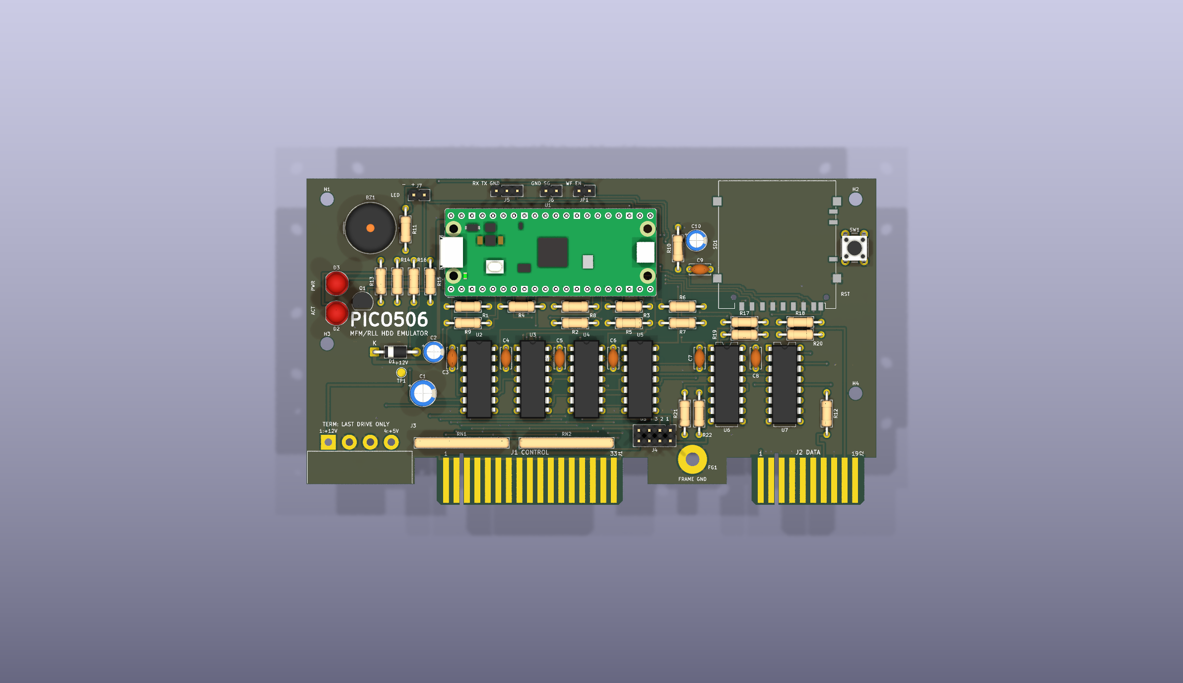 | 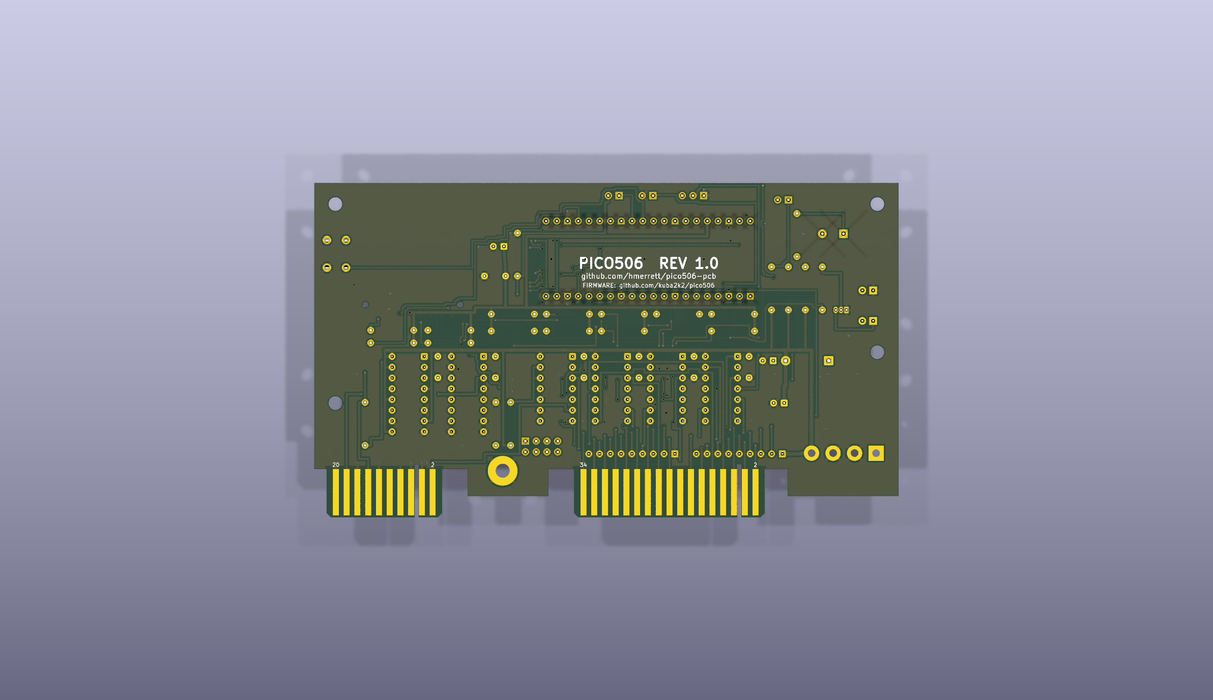 |
Also in doc/: an isometric render, front/back layer PDFs, gerbers +
Excellon (pico506-gerbers.zip), a CSV BOM and a placement file. The schematic
PDF is pico506-sch.pdf.
36 line items, 62 parts, nothing surface-mount and nothing exotic. Quantities
and designators below are generated from the schematic — the machine-readable
copy is doc/pico506-bom.csv.
| Ref | Qty | Value | Notes |
|---|---|---|---|
| U1 | 1 | Raspberry Pi Pico | Pico or Pico W, THT header or castellated. The footprint takes either. |
| U2, U3 | 2 | 74LS05 | Hex inverter, open collector. Not 7404 — the open-collector output is what lets the terminated 5 V bus idle high. |
| U4, U5 | 2 | 7438 | Quad NAND, open collector, buffered. Plain 7438 (or 74S38) is preferred over 74LS38: the LS part sinks 24 mA where the bus wants 40 mA to hold a 220/330-terminated line at a valid low. 74LS38 will usually work with one drive on a short cable; use 7438 if you want spec margin. |
| U6 | 1 | AM26LS31CN | Quad RS-422 differential driver (READ data out). |
| U7 | 1 | MC3486N | Quad RS-422 differential receiver (WRITE data in). AM26LS32AC is a drop-in alternative and is usually easier to find. |
| Q1 | 1 | 2N3904 | LED sink for the front-panel activity LED. Any small NPN. |
| D1 | 1 | 1N5817 | Schottky, feeds the Pico's VSYS from +5 V. A 1N5819 or SS14-class part is fine; don't substitute a plain 1N400x — the forward drop leaves too little VSYS headroom. |
| D2 | 1 | LED 5 mm amber | ACT — activity. |
| D3 | 1 | LED 5 mm green | PWR — power. |
| Ref | Qty | Value | Notes |
|---|---|---|---|
| RN1 | 1 | 220 Ω SIP-9 | Terminator pull-up half. Bourns 4609X-101-221 (bussed, 8 resistors, common pin 1). Fit in a 9-pin SIP socket — see Termination. |
| RN2 | 1 | 330 Ω SIP-9 | Terminator pull-down half. Bourns 4609X-101-331. Also socketed. |
| R21 | 1 | 220 Ω | Fixed 220/330 divider on the selected drive-select line, after the J4 jumper — the way an ST-225 does it. Not removable. |
| R22 | 1 | 330 Ω | ” |
| R1–R9, R16 | 10 | 1 kΩ | R1–R9 pull the 74LS05 open-collector outputs up to +3V3 for the Pico. R16 is the PWR LED resistor. |
| R10, R14, R15 | 3 | 470 Ω | R10 is the WRITE FAULT input pull-up; R14/R15 are the ACT LED resistors (on-board and front-panel). |
| R11, R12 | 2 | 100 Ω | R11 buzzer series, R12 terminates the WRITE differential pair across U7's inputs. |
| R13 | 1 | 4.7 kΩ | Q1 base. |
| R17–R20 | 4 | 10 kΩ | SD card SPI pull-ups. |
| C1 | 1 | 100 µF 16 V | Bulk on +5 V. Radial, 6.3 mm body, 2.5 mm pitch. |
| C2 | 1 | 22 µF 16 V | Bulk on VSYS. Radial, 5 mm body. |
| C3–C9 | 7 | 100 nF | Ceramic disc, 5 mm pitch. One per logic IC (C3–C8) plus one for the SD socket (C9). |
| C10 | 1 | 10 µF 16 V | +3V3 bulk next to the SD socket. |
All resistors are 1/4 W axial on a 10.16 mm (0.4 in) footprint — the classic DIN0207 body with the leads bent out, so they lie flat.
| Ref | Qty | Part | Notes |
|---|---|---|---|
| J1 | — | ST-506 control, 34-pin card edge | Etched into the board. Mates a 3M 3463 / AMP 88373-3 style IDC card-edge socket. |
| J2 | — | ST-506 data, 20-pin card edge | Etched into the board. Mates 3M 3461 / AMP 88373-6. |
| J3 | 1 | AMP/TE 350211-1 4-pos MATE-N-LOK | Cable side is AMP 1-480424-0 with 350550-series pins. This is the standard 4-pin drive power connector. The footprint expects the vertical header with its legs formed 90° for rear entry — exactly what Seagate did — or use a right-angle MATE-N-LOK equivalent. |
| FG1 | 1 | AMP 61761-2 faston tab | Frame ground, 0.187 in tab, 3.3 mm hole. Or just bolt a ring lug through it. |
| SD1 | 1 | Hirose DM1AA-SF-PEJ(82) | Full-size push-push SD socket. The card ejects over the board's front edge. |
| SW1 | 1 | 6 mm tactile switch, 4.3 mm | RST — pulls the Pico's RUN low. |
| J4 | 1 | 2×4 pin header, 2.54 mm | Drive select. See Straps. |
| J5 | 1 | 1×3 pin header | UART console: GND / TX / RX. |
| J6 | 1 | 1×2 pin header | SERVO GATE — 3.3 V logic, JVC RLL drives only. |
| J7 | 1 | 1×2 pin header | Front-panel activity LED: pin 1 anode, pin 2 cathode. |
| JP1 | 1 | 1×2 pin header | WF EN — WRITE FAULT enable. |
| TP1 | 1 | test pad | +12 V, so you can confirm the rail without probing the connector. |
| H1–H4 | 4 | M3 | 3.2 mm mounting holes. |
| — | 6 | DIP socket | 4 × DIP-14, 2 × DIP-16. Optional but recommended. |
| — | 2 | SIP-9 socket | For RN1/RN2, so the terminator can come out. Not optional if this drive might sit mid-chain. |
The silkscreen reads DS 4 3 2 1 left to right (west to east). Each column is
one J1 drive-select line on its odd pin and the shared DS_SEL_N node on its
even pin; fitting a shunt across one column selects that drive address.
Fit exactly one shunt.
| Column | J1 pin | Selects |
|---|---|---|
1 (east) | 26 | DS1 |
2 | 28 | DS2 |
3 | 30 | DS3 |
4 (west) | 32 | DS4 |
Which one you want depends on your controller's cable. With a straight-through control cable, the first drive is DS1. With an IBM-style twisted control cable the twist reassigns the select lines between the two drive connectors, and the drive on the end (twisted) connector wants DS2 — that is the intended default for this board. Check your controller's manual: this is the single most common reason an otherwise-working drive is not detected.
Downstream of the shunt, DS_SEL_N carries its own fixed 220/330 divider
(R21/R22), matching ST-225 practice — that termination stays fitted regardless
of chain position.
| Header | Fitted | Effect |
|---|---|---|
JP1 WF EN | open (default) | WRITE FAULT is not driven; the line idles inactive via R10. |
JP1 WF EN | closed | Firmware drives WRITE FAULT from GP22. Only close this if your firmware build actually asserts it. |
J6 SERVO GATE | — | 3.3 V SERVO GATE for JVC JD-3824-class RLL drives. Leave unconnected for ordinary MFM. |
J7 FRONT LED | — | Parallels the on-board ACT LED to a panel LED. Pin 1 is the anode. |
J5 UART | — | Console at GND/TX/RX. 3.3 V logic — do not connect a 5 V TTL adapter. |
ST-506 is a daisy chain, and the spec puts a 220 Ω/330 Ω divider on every control input — but only on the drive at the far end of the cable. Every other drive on the chain must have its terminator removed, or the lines are loaded several times over and nothing reads reliably.
That is what RN1 (220 Ω) and RN2 (330 Ω) are, and it is why they belong in sockets:
The silkscreen says TERM: LAST DRIVE ONLY next to them as a reminder. The
data cable (J2) is point-to-point and needs no such choice — the WRITE pair's
terminator (R12) is soldered down.
Both card-edge tabs stand 5 mm proud of the main outline, are 1.6 mm thick, and carry a 0.914 mm key slot routed 12.5 mm in from the tab tip, between pins 4 and 6 — the standard ST-506 keying, so a connector cannot be seated backwards. Odd pins are on the front (F.Cu) face, even pins on the back, at 2.54 mm pitch; fingers are 1.40 mm wide and 11.43 mm long with the copper pulled back 0.45 mm from the routed tip.
The fingers are 11.43 mm long but the tab only stands 5 mm proud, so the board is cut away beside each tab as well — otherwise the mating socket's shell hits the main board edge after 5 mm with two thirds of the finger length still unengaged. Each relief runs inboard to y = 67.57 mm, level with the finger tops, giving a free-standing tongue exactly as long as the gold:
| Relief | Width | Note |
|---|---|---|
| J1 west | 5.34 mm | Limited by the J3 power housing 0.6 mm further west, not by choice — see below. |
| J1 east | 6.00 mm | |
| J2 west | 6.00 mm | |
| J2 east | 2.90 mm | The board simply ends here; the whole south-east corner is removed, so there is nothing east of the J2 tab to foul. |
The overall envelope is unchanged — 138 × 74 mm plus the 5 mm tabs — so this costs nothing mechanically.
Check this against your actual sockets. The J1 relief can only be 5.34 mm wide on its west side, because the J3 power connector housing (a full 1.00 in wide, its east face at x = 25.62 mm) is immediately beyond it. If your J1 socket needs more than that, the obstruction is the power connector body, not the board, and the fix is to shift J3 east — which moves it off the measured ST-225 position.
TAB_RELIEF_Wintools/layout.pyis the single knob for relief width.
Extending the tabs further instead of notching would also work and is a
one-constant change (TAB_PROTRUDE), but it moves every finger pad south,
invalidates all the hand-routed finger escapes, and grows the board's depth
past the drive's rear plane.
Lateral positions follow the measured ST-225 arrangement so ordinary cable dressing just works. Measured from the board's west edge:
| Tab | Centre | Width | Pins |
|---|---|---|---|
| J1 control | 54.10 mm | 45.09 mm | 34 |
| J2 data | 121.45 mm | 27.30 mm | 20 |
J1 uses the ST-506/412 control pinout (even pins signal, odd pins ground); J2
uses the ST-412 data pinout, with the two differential pairs on 13/14 (WRITE)
and 17/18 (READ). Both are enumerated in
tools/netlist.py, which is the single source of truth for
the whole design.
J3 power is the usual 4-pin order: pin 1 = +12 V, pins 2 and 3 ground, pin 4 = +5 V, marked on the silkscreen. +12 V is not used by the emulator — it is brought to TP1 only so you can verify the supply.
Everything below is from tools/layout.py; the origin is the
board's north-west corner viewed from the component side.
RST button are the other two things you will want access
to: USB is at the Pico's west end, RST at the east edge.If you are building an enclosure or a bay adapter: this board is not a mechanical drop-in for a 3.5 in or 5.25 in drive. It reproduces the electrical and connector geometry of an ST-225 rear face, not its chassis. On a real drive the card-edge mid-plane sits roughly 4.8 mm above the bay floor; if you want the cables to land where a drive's would, that is the dimension to match, and SFF-8501 gives the bay hole pattern to mount against. The four holes here are a generic rectangle, not the SFF pattern — pick them up with standoffs.
Two layers, 1.6 mm FR4, 1 oz copper, minimum track 0.2 mm and minimum clearance 0.18 mm — comfortably inside every cheap prototype service's capability. Two things are not default, though, and both matter:
Also: the key slots are 0.914 mm routed slots cut right through, so the fab
needs to treat them as internal routing, not drills — as are the four relief
notches beside the tabs. All of it is on Edge.Cuts; the two plating notes are
written onto the Cmts.User layer of the board so they travel with the gerbers.
Low parts first, and leave the socketed parts until you have tested the rails:
The schematic and board are generated, not hand-drawn —
tools/netlist.py is the single source of truth and both
generators consume it. Do not edit the .kicad_sch or .kicad_pcb by hand;
your changes will be overwritten.
cd tools
python3 gen_sch.py ../pico506.kicad_sch   # schematic (+ writes sch_uuids.json)
python3 gen_footprints.py                 # project footprint library
./check.sh                                # board + zone fill + full DRC
./export.sh                               # renders, PDFs, gerbers, BOM
check.sh regenerates the board, fills the zones, re-stamps the .kicad_pro
(pcbnew's save clobbers it) and runs --severity-all DRC into
drc.txt. It also surfaces the generators' own warnings — a
failed ground link or an unrouted net shows up there long before you notice it
as "unconnected items" in DRC.
Two analysis helpers, both needing KiCad's bundled python
(/Applications/KiCad/KiCad.app/Contents/Frameworks/Python.framework/Versions/Current/bin/python3):
tools/stitch.py — walks the GND pour, unions every ground island with
the tracks, vias and pads that touch it, and reports any fragment the main
plane does not reach, along with a ready-to-paste fix (stitch via, bridge
track, or a pad-to-pad link). This is how the ground plane got from six
orphaned fragments — including floating IC ground pins — to a single
connected plane. Re-run it after any routing or placement change: the
coordinate-based entries in GND_STITCH_VIAS go stale as soon as the maze
router lands differently, and a stale via can end up sitting on a signal
track.tools/place_check.py — reports courtyard boxes and how deeply
overlapping pairs interpenetrate, so a placement nudge can be sized instead
of guessed.GND_STUBS in gen_pcb.py) are routed as
first-class nets inside the router's search, so a pass only counts if the
signals and the ground links both fit. Moving one to a post-routing pass will
silently strand a decoupling cap's ground.router.CLR is 0.24 mm against a 0.18 mm rule. The slack absorbs a
route's closest approach between grid cells. Raising it to 0.25 leaves the
U3/U4 corridor one track short of holding both the signals and C5's ground
rescue; lowering it starts producing real clearance violations.place_references() in
gen_pcb.py), by trying positions around each part and taking the first that
clears every mask aperture, all footprint silk, the board texts and the board
edge. Don't hand-place them — adjust the candidate list instead.lib_footprint_mismatch is set to ignore in the project file. The board
is regenerated from the libraries every build, so "the board copy has drifted
from the library" cannot happen the way it can on a hand-edited board. KiCad
flags U1 anyway; its pads, graphics, zones and attributes all compare
identical, and the residual difference is bookkeeping that survives a pcbnew
load/save round-trip. Every other rule is at its default severity.Longer-form layout history and the routing plan are in
tools/ROUTING_PLAN.md.
The Pico506 emulator is by Kuba Szczodrzyński — kuba2k2/pico506, described at length in Emulating a 1987 proprietary RLL hard drive. That project is the emulator: the firmware, the PIO signal generation, the level-shifter/inverter circuit this board's logic section is a direct descendant of, and the pin assignment the whole layout is wired to. Without it there is nothing to put on a PCB.
What this repository adds is the board itself: the schematic capture, the
two-layer layout, the ST-506 card-edge tabs and their ST-225-derived geometry,
the project footprint library, and the Python generators in
tools/ that produce all of it. Bugs in the board are mine, not
upstream's.
Also drawn on: the ST-506/ST-412 interface pinouts and the 220/330 termination and drive-select conventions from Seagate's ST-225 documentation, and the HDD Clicker for the buzzer idea that upstream implements.
GNU General Public License v3.0 — the same licence as upstream, so the board and the firmware it exists to carry stay under the same terms.
Copyright © 2026 Henry Merrett (this PCB: schematic, layout, footprints and generators). Copyright © 2025 Kuba Szczodrzyński (Pico506, from which this board's circuit is derived).
This is a hardware design under a software licence, which is how upstream is licensed and therefore what a derivative here has to be. In practice: the design files are the "source", and if you fabricate, modify or distribute the board you owe the recipients those files under the GPL. There is no warranty, and note that rev 1.0 has never been fabricated — see the status note at the top.
| Qty | Value | Footprint | References |
|---|---|---|---|
| 10 | 1k | Resistor_THT:R_Axial_DIN0207_L6.3mm_D2.5mm_P10.16mm_Horizontal | R1, R2, R3, R4, R5, R6, R7, R8, R9, R16 |
| 7 | 100n | Capacitor_THT:C_Disc_D5.0mm_W2.5mm_P5.00mm | C3, C4, C5, C6, C7, C8, C9 |
| 4 | 10k | Resistor_THT:R_Axial_DIN0207_L6.3mm_D2.5mm_P10.16mm_Horizontal | R17, R18, R19, R20 |
| 4 | M3 | MountingHole:MountingHole_3.2mm_M3 | H1, H2, H3, H4 |
| 3 | 470 | Resistor_THT:R_Axial_DIN0207_L6.3mm_D2.5mm_P10.16mm_Horizontal | R10, R14, R15 |
| 2 | 100 | Resistor_THT:R_Axial_DIN0207_L6.3mm_D2.5mm_P10.16mm_Horizontal | R11, R12 |
| 2 | 7438 | Package_DIP:DIP-14_W7.62mm | U4, U5 |
| 2 | 74LS05 | Package_DIP:DIP-14_W7.62mm | U2, U3 |
| 1 | +12V | TestPoint:TestPoint_Pad_D2.0mm | TP1 |
| 1 | 100u/16V | Capacitor_THT:CP_Radial_D6.3mm_P2.50mm | C1 |
| 1 | 10u/16V | Capacitor_THT:CP_Radial_D5.0mm_P2.50mm | C10 |
| 1 | 1N5817 | Diode_THT:D_DO-41_SOD81_P10.16mm_Horizontal | D1 |
| 1 | 220 | Resistor_THT:R_Array_SIP9 | RN1 |
| 1 | 220 | Resistor_THT:R_Axial_DIN0207_L6.3mm_D2.5mm_P10.16mm_Horizontal | R21 |
| 1 | 22u/16V | Capacitor_THT:CP_Radial_D5.0mm_P2.50mm | C2 |
| 1 | 2N3904 | Package_TO_SOT_THT:TO-92_Inline | Q1 |
| 1 | 330 | Resistor_THT:R_Axial_DIN0207_L6.3mm_D2.5mm_P10.16mm_Horizontal | R22 |
| 1 | 330 | Resistor_THT:R_Array_SIP9 | RN2 |
| 1 | 4.7k | Resistor_THT:R_Axial_DIN0207_L6.3mm_D2.5mm_P10.16mm_Horizontal | R13 |
| 1 | ACT amber | LED_THT:LED_D5.0mm | D2 |
| 1 | AM26LS31CN | Package_DIP:DIP-16_W7.62mm | U6 |
| 1 | AMP 350211-1 | pico506-lib:PWR_MATE-N-LOK_350211_Horizontal | J3 |
| 1 | DRIVE SELECT | Connector_PinHeader_2.54mm:PinHeader_2x04_P2.54mm_Vertical | J4 |
| 1 | FRAME GND | pico506-lib:Faston_Tab_AMP61761 | FG1 |
| 1 | FRONT LED | Connector_PinHeader_2.54mm:PinHeader_1x02_P2.54mm_Vertical | J7 |
| 1 | MC3486N | Package_DIP:DIP-16_W7.62mm | U7 |
| 1 | PS1240 | Buzzer_Beeper:Buzzer_TDK_PS1240P02BT_D12.2mm_H6.5mm | BZ1 |
| 1 | PWR green | LED_THT:LED_D5.0mm | D3 |
| 1 | RESET | Button_Switch_THT:SW_PUSH_6mm_H4.3mm | SW1 |
| 1 | Raspberry Pi Pico | pico506-lib:RaspberryPi_Pico_Common_THT | U1 |
| 1 | SD socket | pico506-lib:SD_Hirose_DM1AA_SF_PEJ82 | SD1 |
| 1 | SERVO GATE 3V3 | Connector_PinHeader_2.54mm:PinHeader_1x02_P2.54mm_Vertical | J6 |
| 1 | ST-506 CONTROL | pico506-lib:EdgeConn_ST506_J1_34 | J1 |
| 1 | ST-506 DATA | pico506-lib:EdgeConn_ST506_J2_20 | J2 |
| 1 | UART | Connector_PinHeader_2.54mm:PinHeader_1x03_P2.54mm_Vertical | J5 |
| 1 | WF EN | Connector_PinHeader_2.54mm:PinHeader_1x02_P2.54mm_Vertical | JP1 |
immonel/e-runout
This project is used to measure electrical runout by comparing measurements from touching probe sensors and Eddy current probes simultaneously.


transistorfet/computie
A collection of 68k computer projects, including a unix-like operating system written in C that runs on them


raymondh2/CompaqPortableIII
Current PCB Memory Expansion board layout is untested. The backplane for the expansion cards is tested and working.

barberd/coco9511pak
This board is a cartridge for the Tandy Radio Shack TRS-80 Color Computer (CoCo), an 8 bit computer produced between 1980 and 1991. It provides an Arithmetic Processor Unit (APU), the AMD 9511, to the CoCo.


It measures 138 × 79 mm and has 2 copper layers, 1.6 mm thick.
62 parts, built around the AM26LS31CN, 74LS05P-E and MC3486N. The full list of its parts is on this page, with links to each part's symbol and footprint where PCBKit's library has them.
From the hmerrett/pico506-pcb repository on GitHub, at the commit this page was made from: the board is pico506.kicad_pcb and its schematic pico506.kicad_sch. PCBKit opens the board in the browser, with nothing to install.
Its repository publishes it under the GPL-3.0 licence: you may reuse it on that licence's terms (keep the author's notice, and for a copyleft licence share your changes alike).