2 layers29 × 16.5 mm

 hisashin/fiberPCB6
All knowledge memo to make PCB with fiber laser
Test01 is an open-source printed circuit board by hisashin, from the hisashin/fiberPCB repository on GitHub. It is a 2-layer board of 23 × 18 mm with 23 parts on 4 nets, routed with 57 tracks and 10 vias.
Its parts include 9 connectors and 6 resistors.
Let's compare fiberPCB with alternatives.
Gerber Files (Free)
FlatCAM, Gerver->CAM conveter
Latest stable FlatCAM3.5 needs Python2.7. Beta supports Python3 but crush often on Linux. Pip install looks easy but crushed while saving projects. I recommend to use Windows or Docker Ubuntu Desktop.
// Run this command in your terminal
docker run -d -v (where you exported gerbers):/gerbers -v (somewhere to save flatcam projects):/projects -it --name flatcam -p 6080:80 -p 5901:5900  -e VNC_PASSWORD=password -v /dev/shm:/dev/shm dorowu/ubuntu-desktop-lxde-vnc:release-v1.2
// My case
docker run -d -v ~/github/fiberPCB/kicad/fiberPCB:/gerbers -v ~/github/fiberPCB/flatcam:/projects -it --name flatcam -p 6080:80 -p 5901:5900  -e VNC_PASSWORD=password -v /dev/shm:/dev/shm dorowu/ubuntu-desktop-lxde-vnc:release-v1.2

// Connect VNC to vnc://localhost:5901, run these commands in Ubuntu terminal not yours.
apt-get -y update
apt-get -y install sudo wget git unzip

//git clone https://bitbucket.org/jpcgt/flatcam <- it was also 3.5 when I tried on 2021 Jan 25
wget https://bitbucket.org/jpcgt/flatcam/downloads/FlatCAM-8.5.zip
unzip FlatCAM-8.5.zip
cd FlatCAM-8.5
sh setup_ubuntu.sh
python FlatCAM.pypython3 -V (3.5)
// It was 3.5 for me and upgrade to 3.8 was needed in later step. skip here if yours is 3.8
add-apt-repository ppa:deadsnakes/ppa
apt-get -y update
apt-get -y install python3.8
update-alternatives --install /usr/bin/python3 python3 /usr/bin/python3.5 1
update-alternatives --install /usr/bin/python3 python3 /usr/bin/python3.8 2
update-alternatives --config python3 (Choose python3.8)
python3 -V
apt install -y python3.8-distutils python-setuptools python3-pip
pip3 -V (8.1.1)
apt remove python3-pip
python3.8 -m easy_install pip
pip -V (21.0)
apt-get -y update
apt-get -y install python3-pip python-setuptools sudo wget
wget https://bitbucket.org/jpcgt/flatcam/downloads/FlatCAM_beta_8.994_sources.zip
unzip FlatCAM_beta_8.994_sources.zip
cd FlatCAM_beta_8.994_sources
sh setup_ubuntu.sh
python3 FlatCAM.pyEZCAD, laser controller
Fiber Laser
Laminator
UV illuminator
Dry film
My case in Tokyo Japan :
| Item | Price | Shipping | Comment |
|---|---|---|---|
| Fiber Laser | $1,837.44 | $249.81 | 20W JPT 200x200mm DHL8-16days |
| Laminator | $10.64 | $11.12 | Got $1800 worth one as junk. Replaced blown fuse:wink: |
| UV illuminator | $4.73 | $0 | I will line them up for larger PCB |
| Dry film | $19.15 | $0 | VANTIYAUS Zp00088(5m x 30cm) |
| FR-4 | $1.64 | $0 | 1.6t x 75 x 100mm |
| Total | $1873.6 | $260.93 | $2395.46 include shippings |
// TODO Stronger/Wider is not always better
// TODO List confirmed to support 1.6mm thickness
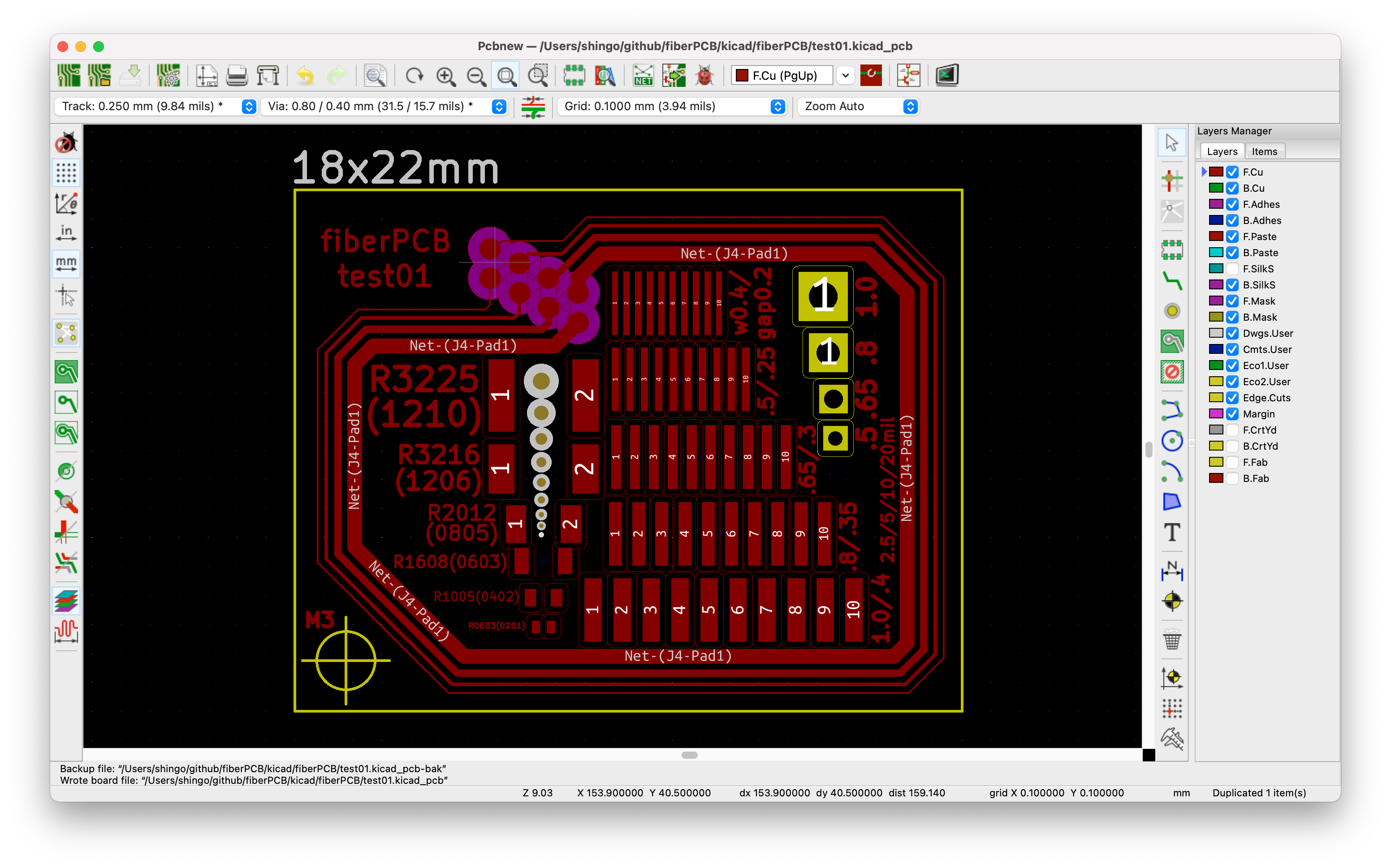
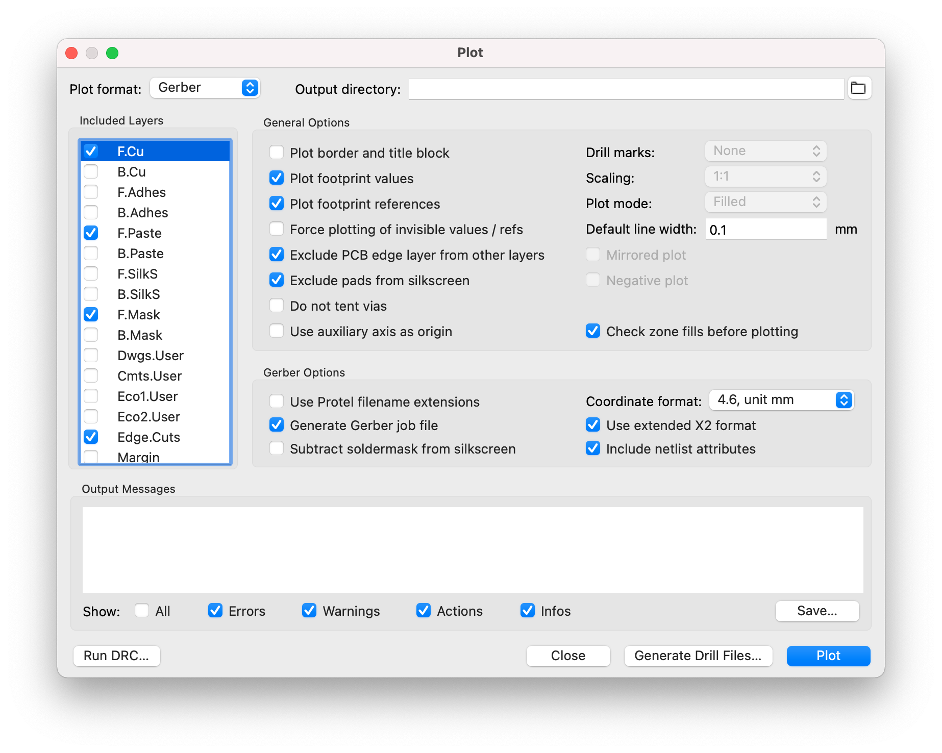
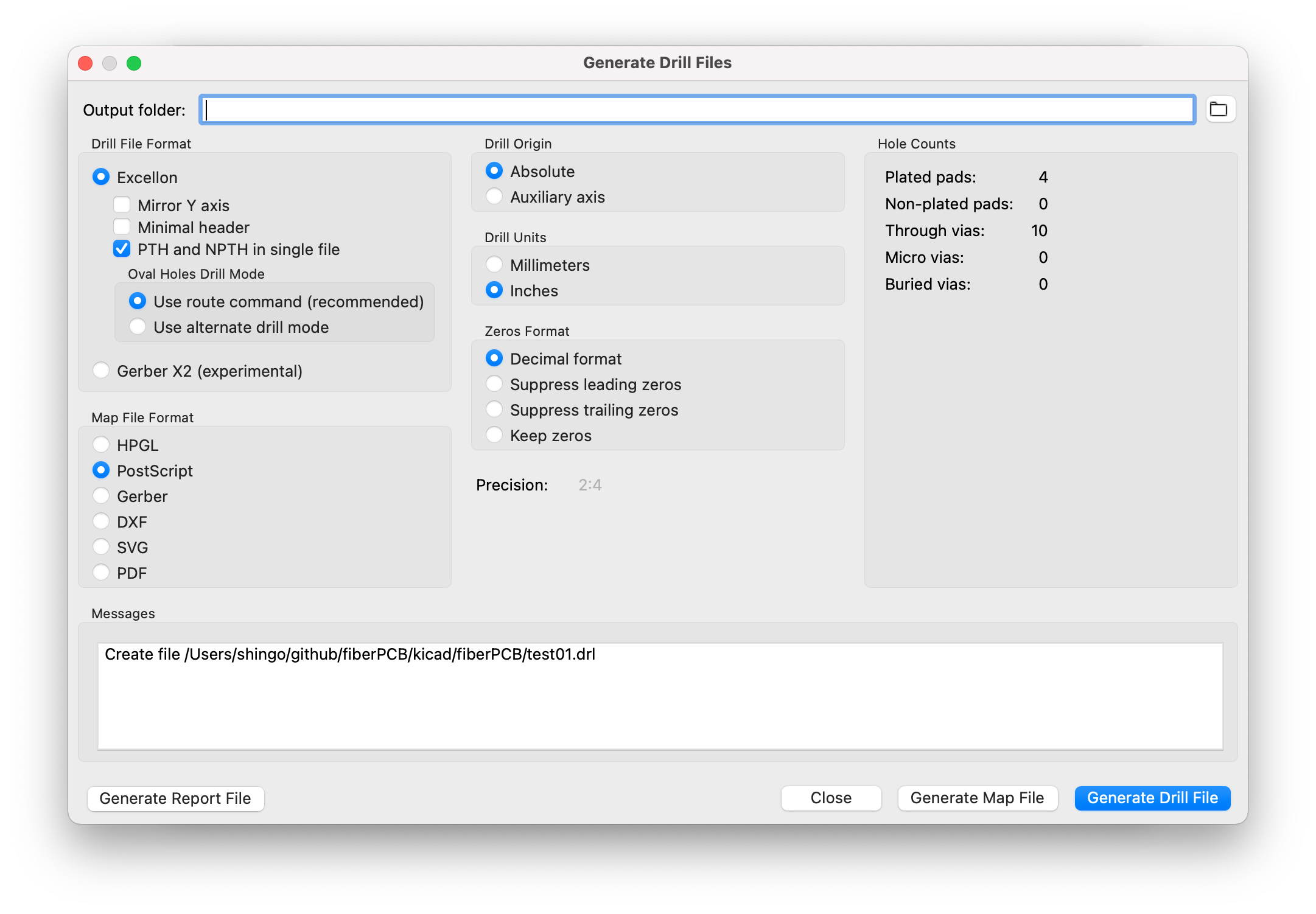
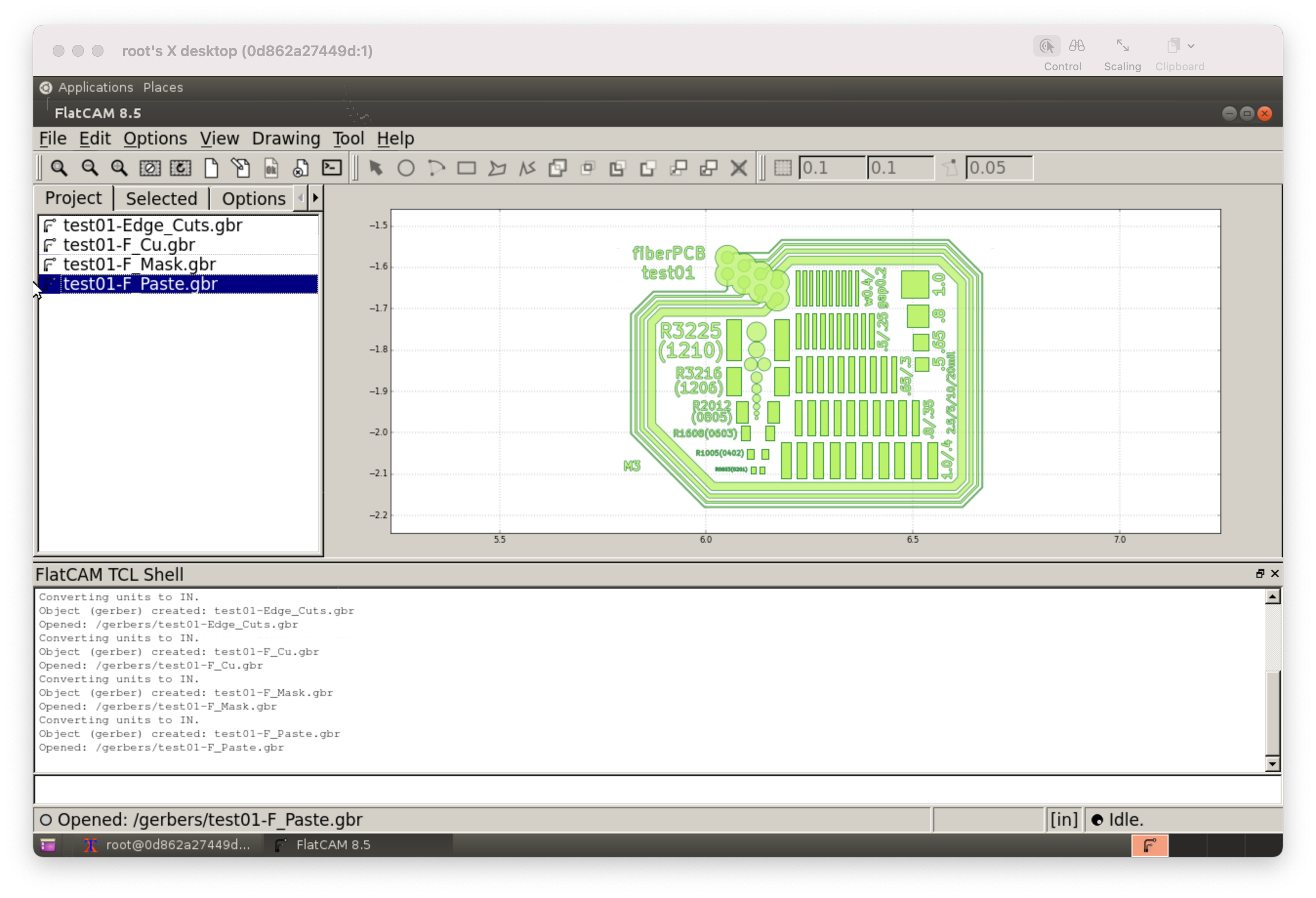
// TODO
| Qty | Value | Footprint | References |
|---|---|---|---|
| 8 | Conn_01x01_Male | fiberPCB:Checkpoint | J1, J2, J3, J4, J5, J6, J7, J8 |
| 1 | Conn_01x01_Male | Pin_Headers:Pin_Header_Straight_1x01_Pitch1.00mm | PH_Pitch1.00 |
| 1 | Conn_01x01_Male | Pin_Headers:Pin_Header_Straight_1x01_Pitch2.00mm | PH_Pitch2.00 |
| 1 | Conn_01x01_Male | Pin_Headers:Pin_Header_Straight_1x01_Pitch2.54mm | PH_Pitch2.54 |
| 1 | Conn_01x01_Male | Pin_Headers:Pin_Header_Straight_1x01_Pitch1.27mm | PH_Pitch1.27 |
| 1 | Conn_01x02_Male | Resistors_SMD:R_0603 | R1608(0603)1 |
| 1 | Conn_01x02_Male | Resistors_SMD:R_1206 | R3216(1206)1 |
| 1 | Conn_01x02_Male | Resistors_SMD:R_0402 | R1005(0402)1 |
| 1 | Conn_01x02_Male | Resistors_SMD:R_0201 | R0603(0201)1 |
| 1 | Conn_01x02_Male | Resistors_SMD:R_1210 | R3225(1210)1 |
| 1 | Conn_01x02_Male | Resistors_SMD:R_0805 | R2012(0805)1 |
| 1 | Conn_01x10_Male | fiberPCB:SOIC-10-0.8-gap0.35 | P.4 |
| 1 | Conn_01x10_Male | fiberPCB:SOIC-10-0.5-gap0.25 | P.2 |
| 1 | Conn_01x10_Male | fiberPCB:SOIC-10-0.65-gap0.3 | P.3 |
| 1 | Conn_01x10_Male | fiberPCB:SOIC-10-1.0-gap0.4 | P5 |
| 1 | Conn_01x10_Male | fiberPCB:SOIC-10-0.4-gap0.2 | P.1 |


google/mozc-devices
Circuit diagrams and firmware source code for Gboard DIY keyboards


Duet3D/Duet-2-Hardware
The KiCAD source for the Duet 3d printer controller see www.duet3d.com
It measures 23 × 18 mm and has 2 copper layers, 1.6 mm thick.
23 parts. The full list of its parts is on this page, with links to each part's symbol and footprint where PCBKit's library has them.
From the hisashin/fiberPCB repository on GitHub, at the commit this page was made from: the board is kicad/fiberPCB/test01.kicad_pcb. PCBKit opens the board in the browser, with nothing to install.
Its repository states no licence, so its author keeps all rights: ask hisashin before reusing the design.