6 layers160 × 120 mm
Pic32main
JuanPoueriet/automatic-spork
Máquina de ruleta física de casino. 6 PCBs: pic32main (cerebro), wheel (rueda de LEDs), displaysa/b/c (paneles de 7 segmentos en cascada) y buttons (botonera).
256 parts

 HeyPCB/hello-8051
HELLO: a tiny 8051 computer shaped like a 1984 desktop. AT89S52, 32 KB SRAM, 128x64 ST7920 LCD, USB-C. 112 x 158 mm 2-layer KiCad 10 board, DRC clean, firmware that writes hello. Built through HeyPCB's MCP server.
Hello is an open-source printed circuit board by HeyPCB, from the HeyPCB/hello-8051 repository on GitHub, published under the MIT licence. It is a 2-layer board of 112 × 158 mm with 27 parts on 47 nets, routed with 392 tracks and 401 vias.
It is built around the AT89S52-24PU, SN74HC573AN and AS6C62256-55PCN, with the C320C104K5R5TA, K330J15C0GF5TL2 and MFR0W4F5101A50 among its other parts. Its parts include 8 capacitors, 5 resistors, 3 ICs, 3 connectors and 2 switches. It belongs with the retro computing and games and lEDs and displays boards and the 8051 (CH55x, STC, AT89) boards of this library.


A 112 × 158 mm 8051 computer shaped like the front of a 1984 desktop machine: the 128×64 LCD sits where the screen would be, the chips sit in the chin, the ISP header sits where the floppy slot was, and a narrower foot runs along the bottom edge.
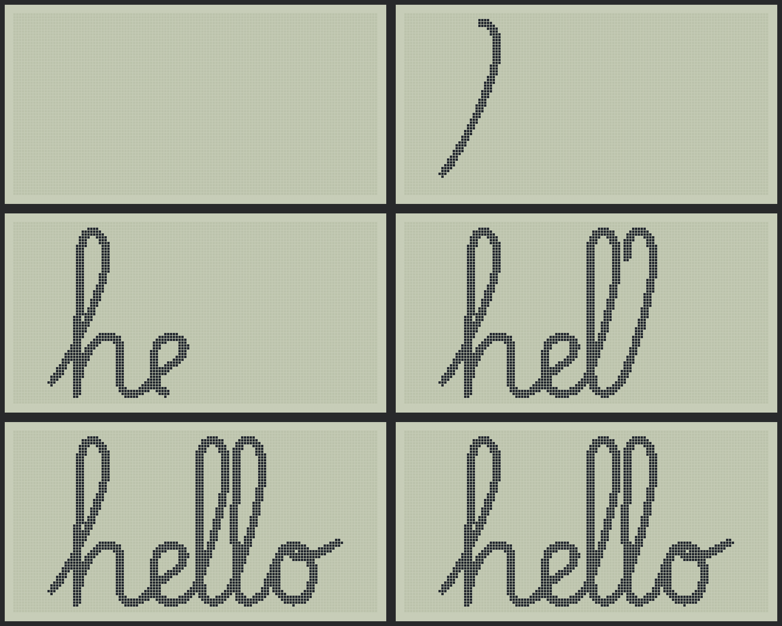
An agent built it through HeyPCB's MCP server, from one prompt to Claude Code: parts, wiring, outline, placement, routing and checks, all as tool calls. It then wrote the firmware, which draws "hello" on the LCD one pen stroke at a time. KiCad 10 opens the files directly, and the board is on Circuit World to open or fork in HeyPCB (sign-in required).
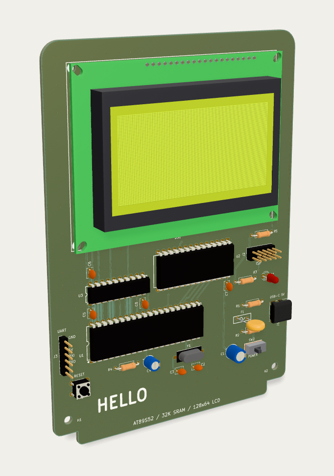
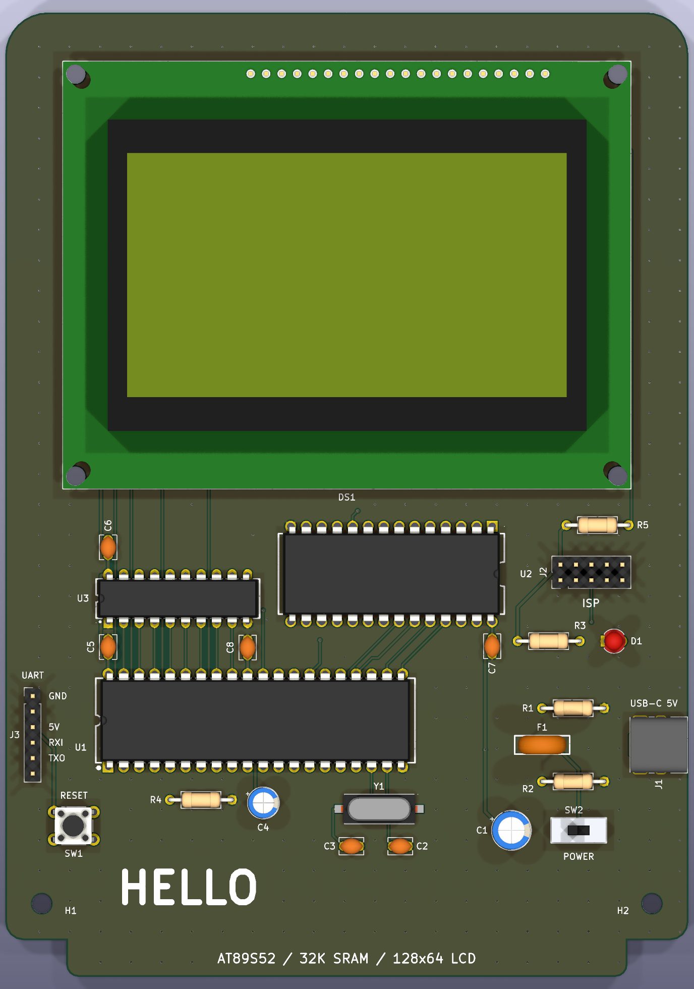
Every part has an LCSC number in the BOM.
firmware/ builds with SDCC (4.6.0 here) and the board's ISP header takes the result:
cd firmware
make        # build/hello.hex, 2,832 of the AT89S52's 8,192 bytes
make sim    # runs the image on a simulated board and renders the screen to build/sim/
hello.hex is in the folder already built. The firmware reads ../hello.svg at build time (tools/svg2c.py), fits its 29 Bézier curves to the panel, then traces them with integer maths, stamping a round pen into a frame buffer in the external SRAM and sending the rows under the pen to the LCD after each of its 1,088 steps.
It has run only in simulation. make sim is a cycle-counted 8051 with a model of the ST7920 wired to P1, written from the ST7920 datasheet's serial protocol. Its final screen matches the bitmap computed from hello.svg with 0 pixels different, and SDCC's own simulator (ucsim) agrees on the frame buffer and the cycle count (4,256,702). That check covers the processor and memory, not the LCD model, so how the HS12864-15C itself handles the panel's bottom half is the first thing to confirm on hardware. The screen's colours in the renders are made up; the pixels are exact.
Measured on this revision:
| Check | Result |
|---|---|
| DRC, KiCad 10.0.6 run locally | 0 errors, 0 unconnected; 27 warnings (14 hole-to-hole, 10 silkscreen over copper, 3 silkscreen near the edge) |
| DRC, HeyPCB | 0 errors, 0 unconnected |
| ERC, HeyPCB | 0 errors |
| ERC, KiCad 10.0.6 run locally | 3 errors, all "input pin not driven" on the SRAM's A0–A2 (below) |
| HeyPCB verify | every rung that ran passed; IR drop and the pin-direction check not verified |
| Fab readiness (JLCPCB) | not ready: no blockers, but HeyPCB could only partly confirm the identity of the through-hole resistors and capacitors, so the BOM has no verdict |
Things to know before ordering:
| Path | What it is |
|---|---|
hello.kicad_pro, .kicad_sch, .kicad_pcb, .kicad_dru | The KiCad 10 project |
heypcb-libs/ | The LCSC parts' symbols and footprints, and one HeyPCB footprint, wired up by fp-lib-table and sym-lib-table |
design.json | The HeyPCB design the schematic and board are generated from |
fab/ | Gerbers and drill files, BOM and pick-and-place (CPL) for JLCPCB |
firmware/ | The SDCC firmware, its simulator, and hello.hex |
hello.svg | The lettering the firmware draws: one pen stroke |
images/ | HeyPCB's 3D view and photograph of the board, the schematic, and the simulated screen |
MIT. See LICENSE.
| Qty | Value | Footprint | References |
|---|---|---|---|
| 4 | 100nF | Capacitor_THT:C_Disc_D3.8mm_W2.6mm_P2.50mm | C5, C6, C7, C8 |
| 2 | 33pF C0G | Capacitor_THT:C_Disc_D3.8mm_W2.6mm_P2.50mm | C2, C3 |
| 2 | 5.1k | Resistor_THT:R_Axial_DIN0207_L6.3mm_D2.5mm_P10.16mm_Horizontal | R1, R2 |
| 2 | MountingHole M3 | MountingHole:MountingHole_3.2mm_M3 | H1, H2 |
| 1 | 100uF 25V | Capacitor_THT:CP_Radial_D6.3mm_P2.50mm | C1 |
| 1 | 10k | Resistor_THT:R_Axial_DIN0207_L6.3mm_D2.5mm_P10.16mm_Horizontal | R4 |
| 1 | 10uF 50V | Capacitor_THT:CP_Radial_D5.0mm_P2.00mm | C4 |
| 1 | 11.0592MHz | HeyPCB_LCSC:HC-49S_L11.4-W4.8 | Y1 |
| 1 | 1k | Resistor_THT:R_Axial_DIN0207_L6.3mm_D2.5mm_P10.16mm_Horizontal | R3 |
| 1 | 22 | Resistor_THT:R_Axial_DIN0207_L6.3mm_D2.5mm_P10.16mm_Horizontal | R5 |
| 1 | 500mA PTC | HeyPCB_LCSC:FUSE-TH_L9.0-W3.0-P5.10-D0.6-S1.10 | F1 |
| 1 | 74HC573 | HeyPCB_LCSC:DIP-20_L26.8-W6.4-P2.54-LS7.6-BL | U3 |
| 1 | AS6C62256 32Kx8 SRAM | HeyPCB_LCSC:PDIP-28_L37.0-W13.5-P2.54-LS15.6-BL | U2 |
| 1 | AT89S52-24PU | HeyPCB_LCSC:DIP-40_L52.3-W13.9-P2.54-LS15.2-BL | U1 |
| 1 | ISP | Connector_PinHeader_2.54mm:PinHeader_2x05_P2.54mm_Vertical | J2 |
| 1 | LCD 128x64 ST7920 | HeyPCB_LCSC:LCD-TH_HS12864-15C | DS1 |
| 1 | POWER | HeyPCB_LCSC:SW-TH_3P-L8.8-W3.9-P2.50_SS12D00G3 | SW2 |
| 1 | RESET | HeyPCB_Verified:TACT600X600P650X450N | SW1 |
| 1 | UART | Connector_PinHeader_2.54mm:PinHeader_1x06_P2.54mm_Vertical | J3 |
| 1 | USB-C (power) | Connector_USB:USB_C_Receptacle_GCT_USB4085 | J1 |
| 1 | red | LED_THT:LED_D3.0mm | D1 |
It measures 112 × 158 mm and has 2 copper layers, 1.6 mm thick.
27 parts, built around the AT89S52-24PU, SN74HC573AN, AS6C62256-55PCN and C320C104K5R5TA. The full list of its parts is on this page, with links to each part's symbol and footprint where PCBKit's library has them.
From the HeyPCB/hello-8051 repository on GitHub, at the commit this page was made from: the board is hello.kicad_pcb and its schematic hello.kicad_sch. PCBKit opens the board in the browser, with nothing to install.
Its repository publishes it under the MIT licence: you may reuse it on that licence's terms (keep the author's notice, and for a copyleft licence share your changes alike).
JuanPoueriet/automatic-spork
Máquina de ruleta física de casino. 6 PCBs: pic32main (cerebro), wheel (rueda de LEDs), displaysa/b/c (paneles de 7 segmentos en cascada) y buttons (botonera).

Ismael034/ulp_daughterboard
KiCad project files for a hardware CTF challenge used during the 2026 ULP CTF. The board is meant to be used with the ch32v203-dev development board.

baldengineer/bit-preserve
Project for capturing vintage, classic, aka old computer schematics in KiCad.


devkyber/PCB
AI-assisted PCB engineering for native KiCad: source evidence, scoped changes, checked previews, human review, and reproducible release packages.

dtatum7/WaCS-52KX
Control board upgrade for a 13.8 V 50 A linear bench power supply


laforestlabs/KiCraft
KiCad PCB automation toolkit — placement, routing, scoring, and experiment management