
2 layers36 × 34 mm
 hennichodernich/patchloop39
Design files for the PatchLoop PCB(s)
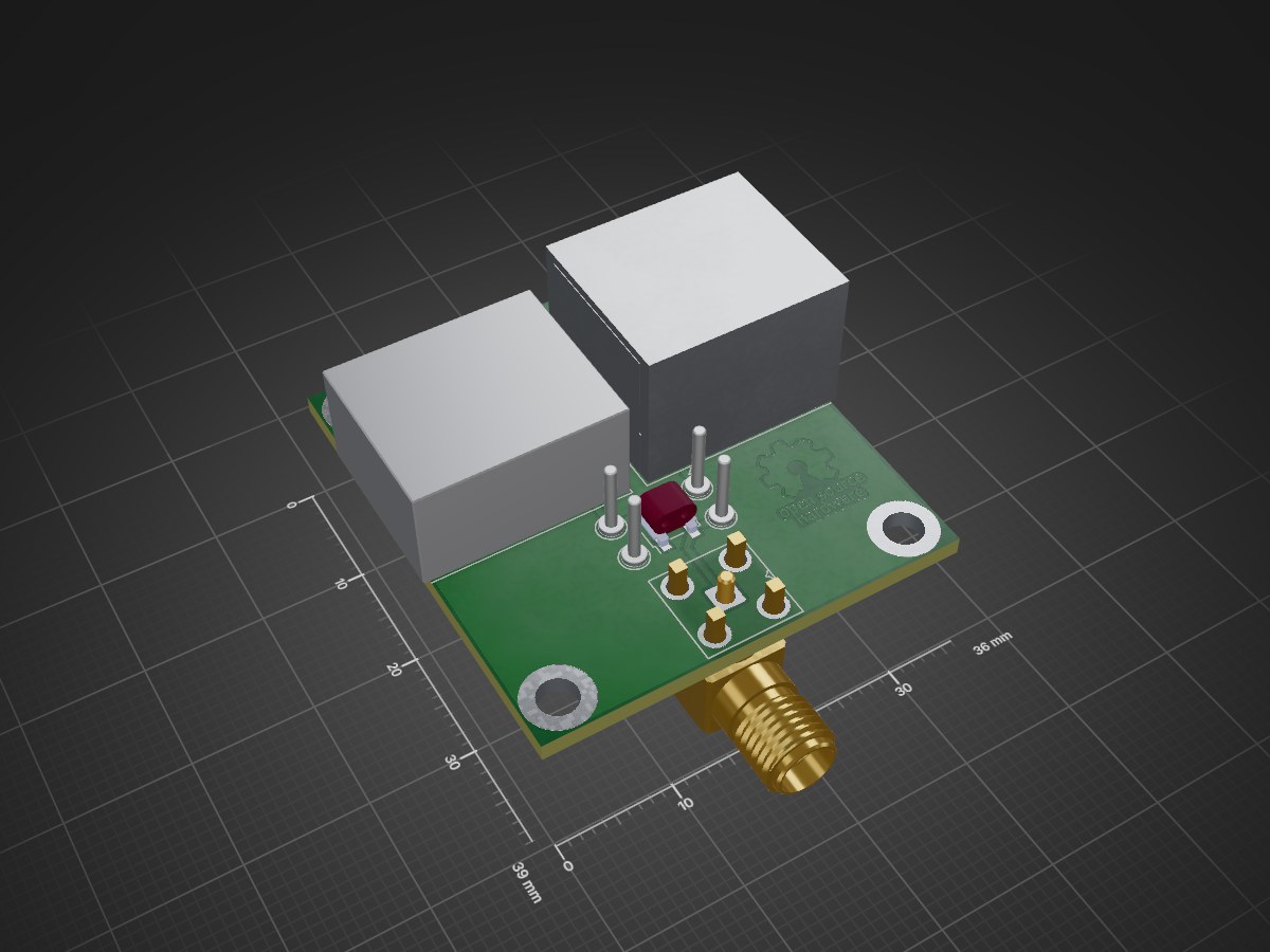
Patchloop is an open-source printed circuit board by hennichodernich, from the hennichodernich/patchloop repository on GitHub. It is a 2-layer board of 36 × 39 mm with 13 parts on 11 nets, routed with 41 tracks and 0 vias.
It is built around the ETC4-1-2TR.
Design files for the PatchLoop PCB
The files patchloop2.kicad_* contain the version with RJ45 jacks on opposite sides. This allows for neat short traces between the jacks.
I needed to rework the files patchloop.kicad_* (jacks on same side) because the first version contained a bug so that only one loop was used effectively.
PCB manufacturer Aisler will directly accept the KiCad file for manufacturing, but you can find zipfiles with the gerbers for both variants in the gerbers/ subdirectory. Any PCB manufacturer (e.g. BetaLayout, JLCPCB, PCBWay, OSHPark) should be able to accept those.
Licensed under CC BY-SA 3.0
While in the schematic (and in the BOM) you will find an M/A-COM ETC4-1-2, this might not be the optimal choice for all possible patch cables. For cables with a length of 2-3 meters, an ETC1-1-13 usually works better to achieve ~50 ohms on the coax connector. The ETC4-1-2 is advantageous for very long cables (and thus higher impedances). I also tried Coilcraft WBC4-4 to transform from very low impedances to 50 ohms (take care of its orientation), but this only makes sense for very short cables: A 1m cable exposed approximately 10 ohms to my NanoVNA.
In general the same holds for selfwound baluns, an 1:1 balun will work best in most of your applications. For instance, I found 2:2 turns on a 9ct Fair-Rite 2843002402 binocular core working well.
Best overall performance including VLF and LF showed a M/A-COM ETC1-1T-2TR combined with 2m of S/FTP Cat6 cable.
| Qty | Value | Footprint | References |
|---|---|---|---|
| 4 | MountingHole_Pad | MountingHole:MountingHole_3.2mm_M3_DIN965_Pad | H1, H2, H3, H4 |
| 4 | TestPoint | TestPoint:TestPoint_THTPad_D2.0mm_Drill1.0mm | TP1, TP2, TP3, TP4 |
| 2 | 8P8C | Connector_RJ:RJ45_Amphenol_54602-x08_Horizontal | J1, J3 |
| 1 | Conn_Coaxial | Connector_Coaxial:SMA_Amphenol_901-143_Horizontal | J2 |
| 1 | ETC4-1-2 | Transformer_SMD:Transformer_MACOM_SM-22 | TR1 |
The 12 most common of 13 parts.
It measures 36 × 39 mm and has 2 copper layers, 1.6 mm thick.
13 parts, built around the ETC4-1-2TR. The full list of its parts is on this page, with links to each part's symbol and footprint where PCBKit's library has them.
From the hennichodernich/patchloop repository on GitHub, at the commit this page was made from: the board is patchloop.kicad_pcb and its schematic patchloop.kicad_sch. PCBKit opens the board in the browser, with nothing to install.
Its repository states no licence, so its author keeps all rights: ask hennichodernich before reusing the design.


samyk/magspoof
A portable device that can spoof/emulate any magnetic stripe, credit card or hotel card "wirelessly", even on standard magstripe (non-NFC/RFID) readers.

fossasia/pslab-scripts
Pocket Science Lab - Scripts for Sensor Experiments


willem-pennings/balancing-cube
A cube that balances itself in a corner or edge using reaction wheels

VoronDesign/Voron-Hardware
Cool Hardware designed by the Voron Design group

hoglet67/RGBtoHDMI
Bare-metal Raspberry Pi project that provides pixel-perfect sampling of Retro Computer RGB/YUV video and conversion to HDMI