
2 layers126.6 × 21.4 mm
ADBv2
mattchesters/zmk-apple-desktop-bus-keyboard
ZMK shield for Apple Desktop Bus Keyboard
17 parts168MIT

 Hawthman/Normkey1
Split daisy-chainable 24/48/72 key keyboard
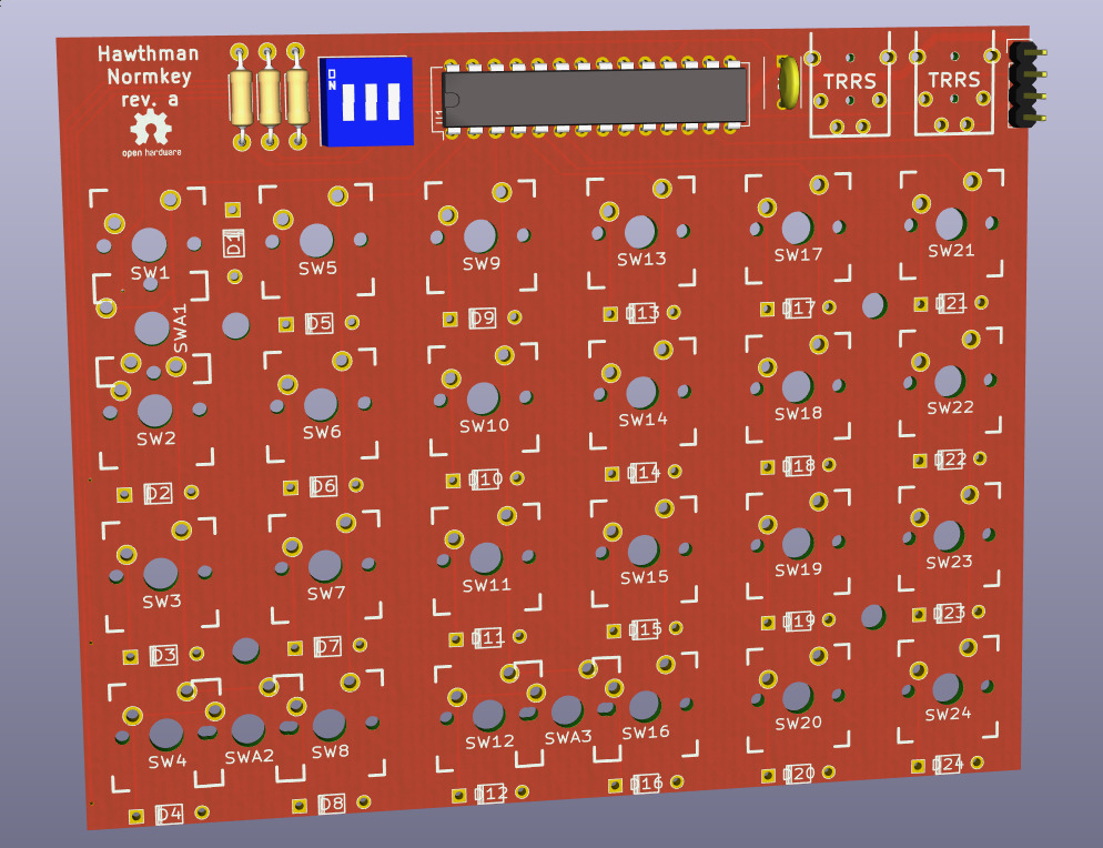
Hawthman is an open-source printed circuit board by Hawthman, from the Hawthman/Normkey repository on GitHub. It is a 2-layer board of 114.3 × 91.4 mm with 65 parts on 49 nets, routed with 239 tracks and 4 vias.
It is built around the MCP23017-E/SS. Its parts include 24 diodes, 24 switches, 3 resistors, 3 connectors and 1 capacitor.
A custom 48 key split keyboard.
| Qty | Value | Footprint | References |
|---|---|---|---|
| 24 | D | Keyboard:DIODE | D1, D2, D10, D11, D12, D13, D14, D15, D16, D17, D18, D19, D20, D21, D22, D23 +8 |
| 24 | SW_PUSH | Keyboard:CHERRY_PCB_100H | SW1, SW2, SW10, SW11, SW12, SW13, SW14, SW15, SW16, SW17, SW18, SW19, SW20, SW21, SW22, SW23 +8 |
| 3 | 10k | Resistors_ThroughHole:Resistor_Horizontal_RM10mm | R1, R2, R3 |
| 3 | SW_PUSH | Keyboard:CHERRY_PLATE_200H | SWA1, SWA2, SWA3 |
| 2 | TRRS | ergodox:4pin35mmAudio | J1, J2 |
| 1 | 0.1uF | Capacitors_ThroughHole:C_Disc_D6_P5 | C1 |
| 1 | DIP3 | Buttons_Switches_ThroughHole:SW_DIP_x3_Slide | SW_DIP1 |
| 1 | MCP23017 | Housings_DIP:DIP-28_W7.62mm | U1 |
| 1 | Test | Pin_Headers:Pin_Header_Straight_1x04 | J3 |
The 60 most common of 65 parts.
It measures 114.3 × 91.4 mm and has 2 copper layers, 1.6 mm thick.
65 parts, built around the MCP23017-E/SS. The full list of its parts is on this page, with links to each part's symbol and footprint where PCBKit's library has them.
From the Hawthman/Normkey repository on GitHub, at the commit this page was made from: the board is pcb/hawthman.kicad_pcb. PCBKit opens the board in the browser, with nothing to install.
Its repository states no licence, so its author keeps all rights: ask Hawthman before reusing the design.
mattchesters/zmk-apple-desktop-bus-keyboard
ZMK shield for Apple Desktop Bus Keyboard

ZeroPhone/ZeroPhone-PCBs
PCB files for ZeroPhone - for gerbers and schematics, go to "Releases" tab!

ktec-hq/ErgoDone
ErgoDox using pro micro. Original work by Dox. Brainhole association present


djbristow/RAILS
RAILS is a software model and implementation of an automated system to assist the model railroader achieve realism in the operation of a model railroad. The model then drives the development of software.


