2 layers20.5 × 53 mm
 hansliss/SensibleRAM
A RAM expansion to make your VIC-20 memory map more sensible
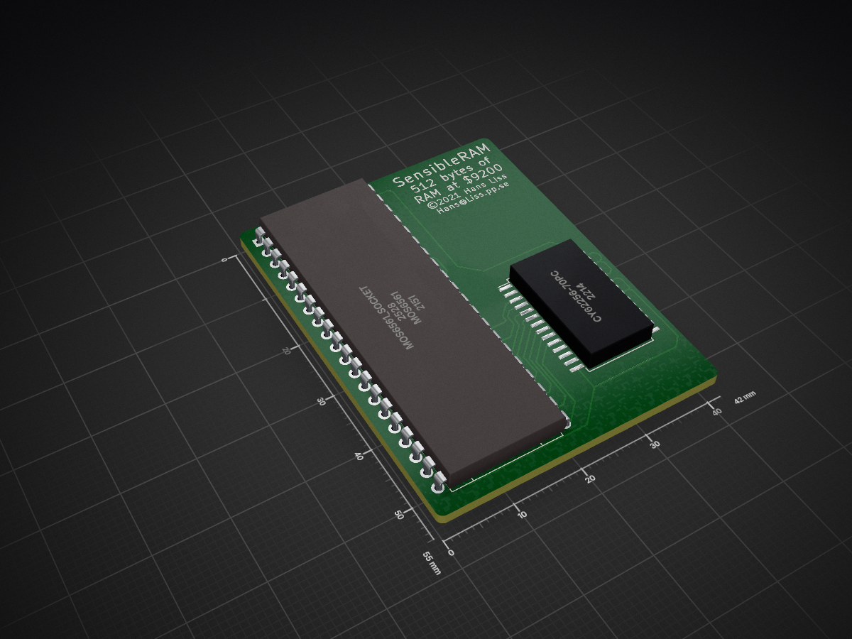
SensibleRAM is an open-source printed circuit board by hansliss, from the hansliss/SensibleRAM repository on GitHub. It is a 2-layer board of 42 × 55 mm with 5 parts on 41 nets, routed with 295 tracks and 17 vias.
It is built around the SN74LVC1G10DBVR and SN74LVC1G27DBVR.

A RAM expansion to make your VIC-20 more sensible
This is actually how the VIC-20 should have been designed in the first place, hence the name SensibleRAM. It would have saved us all some headaches back in the day.
You may already know that there are many different cool modern memory expansion cartridges for the VIC-20 nowadays, providing up to 35-37kB of expansion memory. Some of that memory can benefit from this hack if you are using BASIC, whilst some of it is not relevant here. The aim here is to provide BASIC with as much memory as possible, regardless of what memory expansions you have.
Before you spend a lot of time on this, please be aware that this is anachronistic nerdery of the highest degree. What this does would have been really cool in 1981. Forty years later, in 2021, not so much.
Note that this hardware is as yet untested. The software has been tested in a patched VICE, however. Once I receive the boards and can test it properly, I'll update this and add some photos.
The VIC-20 has a somewhat confusing memory map. It comes with 5kB of system RAM as standard, with 1k at the bottom of the memory map, and 4k at $1000. To BASIC, those upper 4k are available as working memory, minus 0.5k that is used by the system for screen memory.
Normally, the screen memory is located at $1E00, so BASIC memory is $1000-$1DFF which is 3584 bytes. One byte is always consumed by BASIC, so the computer reports 3583 bytes free.
If you add a 3k RAM expansion, it will be located at $0400-0FFF, and the available space increases to 6655 bytes.
If you add larger expansions, they will start att BLK1 at $2000 and expand upwards until they reach $7FFF. However, when this happens, the screen memory becomes a problem, since at $1E00, it will split the system RAM in two non-contiguous parts. That won't do, so the screen memory is moved to $1000 if you add memory to BLK1, and all the memory between $1200 and $7FFF becomes usable to BASIC.
However, with one of those larger expansions in place, any 3k memory at $0400 becomes unusable to BASIC, since it ends up outside the contiguous area.
All this has two negative effects on the system:
The reason that the screen memory is located in one of those places as opposed to $0400 or $7E00 is the way the VIC chip is wired into the system. The screen memory has to be shared between the CPU and the VIC, and the VIC can only address 16k of memory.
The way this has been handled is that the VIC chip shares two different blocks with the CPU, BLK0 and BLK4. The VIC chip has 14 address bits. VA0-VA12 are connected via a tri-state buffer (controlled by a clock pin, but let's leave bus sharing out of this) to the CPU's CA0-CA12, but the most significant bit VA13 is connected to the active-low block selector /BLK4. This means that what the CPU sees as $0000-$1FFF, the VIC sees as $2000-$3FFF, and what the CPU sees as $8000-$9FFF is $0000-1FFF to the VIC.
There's also a mechanism explicitly blocking the VIC chip from sharing some areas with the CPU. Those include the three RAM blocks RAM[1-3] at $0400, the main expansion and ROM blocks BLK[1,2,3,5,6,7] (which have to be blocked since the VIC chip can't address them), and the two auxiliary I/O areas I/O2 and I/O3, located within BLK4. On top of that, the expansions we talked about earlier are all cartridge expansions, so they are sitting on the CPU bus rather than the VIC bus, which means they are unavailable to the VIC anyway.
So, we're left with choosing an area within the interval $1000-$1FFF for the screen memory, since the first kB in BLK0 is used by the OS (although you can map the screen memory to the zero page, for a fun exercise), and BLK4, which is used only for the character ROM, the colour RAM and the I/O registers, doesn't have any available RAM.
Tough.
However, the I/O registers at I/O0 ($9000-$93FF) take up far less than the entire interval, with the highest register at $912F. This leaves $9200-$93FF entirely free, and this area is addressable to both the CPU and the VIC.
So, this project adds 512 bytes of RAM to $9200, and with the included programs you can move the screen memory to this area on your VIC, freeing up 512 bytes of BASIC RAM. If you have both 3k and 8k+ expansions, you can also add those 3k to your available BASIC RAM, for a whopping total win of 3500 bytes.
The included assembly program will try to move the screen memory and start/end memory pointers as correctly as possible regardless of what memory expansions are present, and will then reinitialize BASIC.
Here's a short BASIC program that does the same, but assumes you have expansions in RAM[1-3] and BLK[1-3]:
10pO36866,pE(36866)or128:pO36869,(pE(36869)and15)or(4*16)
20pO648,146:pO44,4:pO43,1:pO56,128:pO55,0:pO642,4
30pO641,0:pO644,128:pO643,0:pO1024,0:sys58232Here are some examples of what happens when you use this with different expansions:
| Expansion | Orig. free ram | Orig max array size | New free RAM | New max array size | RAM increase |
|---|---|---|---|---|---|
| None | 3583 | 1119 | 4095 | 1289 | 512 |
| RAM[1-3] | 6655 | 2143 | 7167 | 2313 | 512 |
| BLK1 | 11775 | 3848 | 12287 | 4021 | 512 |
| RAM[1-3], BLK1 | 11775 | 3848 | 15359 | 5043 | 3584 |
| BLK[1-2] | 19967 | 6581 | 20479 | 6751 | 512 |
| RAM[1-3], BLK[1-2] | 19967 | 6581 | 23551 | 7774 | 3584 |
| BLK[1-3] | 28159 | 9310 | 28671 | 9480 | 512 |
| RAM[1-3], BLK[1-3] | 28159 | 9310 | 31743 | 10505 | 3584 |
The "max array size" fields come from an experiment I did, using the BASIC program testmem.bas that DIM'd string arrays of increasing size and filled them with strings, until no more memory was left. This program would have taken a week to run at the largest memory sizes, had I not run it in warp mode in VICE (see VICE_patching_notes.md).
Feel free to build on this! One possible addition would be to add an I/O location at, say $91FF, that causes the character ROM to be detached from the CPU bus and replaced with RAM, for an additional 4k of available RAM at $8000 - $8FFF, which is within the contiguous section. This would increase free space to 35839 bytes. Since this design uses a 32k chip which is 99.4% wasted, this would be a noble use of some of the space.
Please let me know what you come up with, and let me know if you actually try this thing out.
bit 7 of $9002 controls A9 of screen memory and A9 of color memory
bit 4-7 of $9005 controls A10-A13 of VIC screen memory. A13 is /BLK4 to the CPU

$9200 = 1001 0010 0000 0000 = (VIC) b01001 000000000
$93FF = 1001 0011 1111 1111 = (VIC) b01001 111111111

!(A9 & A12 & !(A10 | A11 | A13))

A9:
$9002.7 = 1

A10-13:
$9005.4-7 = 0100
§1
| Qty | Value | Footprint | References |
|---|---|---|---|
| 1 | CY62256-70PC | VIC-20:SOP-28W_330mil_Pitch1.27mm | U5 |
| 1 | MOS6561 | Housings_DIP:DIP-40_W15.24mm | U2 |
| 1 | MOS6561_socket | Housings_DIP:DIP-40_W15.24mm | U1 |
| 1 | SN74LVC1G10DBVR | TO_SOT_Packages_SMD:SOT-23-6_Handsoldering | U4 |
| 1 | SN74LVC1G27DBVR | TO_SOT_Packages_SMD:SOT-23-6_Handsoldering | U3 |

OUXT-Polaris/plug-in-supply-distributor
PCB design files for a power distribution board that plugs into a base board.

GOROman/gbc-rp2350b-romcart
R0 review draft: RP2350B/Core2350B2 Game Boy cartridge carrier, KiCad/BOM/Gerber; not fabrication-ready

DD1SB/ARDF-TX
Date: 2026-10-15. Engineering review only; unbuilt and unenergized. Open RF80.kicadpro, schematic and native PCB in KiCad10.0.6. Three primary PCBs and the separate VHF true-AM design are unchanged.


joypad-ai/joypad-os
Universal controller firmware for building adapters, dongles, and custom controllers.

OLIMEX/OLINUXINO
OLINUXINO is Open Source / Open Hardware, low cost from EUR 24 Linux Industrial grade Single Board Computer capable to operate -25+85C

jamro/tiny-engineer
A small desktop robot that brings an AI coding assistant to life, physically acting out when it reads files, thinks, writes code, and finishes work.

hackclub/OnBoard
💡 Join 1,000 teenagers and make your first PCB with a $100 grant!
It measures 42 × 55 mm and has 2 copper layers, 1.6 mm thick.
5 parts, built around the SN74LVC1G10DBVR and SN74LVC1G27DBVR. The full list of its parts is on this page, with links to each part's symbol and footprint where PCBKit's library has them.
From the hansliss/SensibleRAM repository on GitHub, at the commit this page was made from: the board is PCBs/SensibleRAM/SensibleRAM.kicad_pcb. PCBKit opens the board in the browser, with nothing to install.
Its repository states no licence, so its author keeps all rights: ask hansliss before reusing the design.