2 layers142.5 × 106.4 mm
 gpgreen/py32_dev8
puya py32 cortex m0 development board
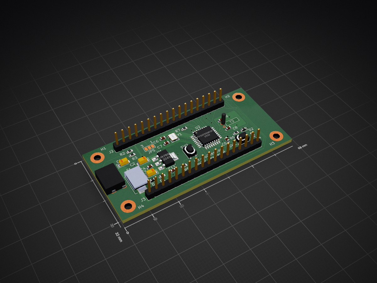
Py32 dev is an open-source printed circuit board by gpgreen, from the gpgreen/py32_dev repository on GitHub, published under the MIT licence. It is a 2-layer board of 68 × 32 mm with 34 parts on 38 nets, routed with 256 tracks and 25 vias.
Its parts include 10 capacitors, 7 resistors, 3 connectors, 2 ICs and 2 diodes. It belongs with the microcontroller boards boards of this library.
KiCad design for a ARM Cortex-M0+ development board. The MCU is a Puya PY32 Series. The specific part is PY032F030K18T6. This can run at a maximum of 48 MHz, and has 8 kbyte SRAM and 64 kbyte Flash. A USB C connector provides 5V power only to the development board. The board must be programmed with a debugger. External crystals are laid out for the MCU to use a 32.768 kHz low speed crystal or a 24 MHz high speed crystal. There is an onboard LDO that provides 500mA of power at 3.3V. A resettable fuse protects the USB port from a short. There is an LED and push button connected to 2 of the GPIO pins. The value of the BOOT0 pin can be set to ground or 3.3V permanently via the solder bridge. A jumper can be used on the pin rails in lieue of the solder bridge. All available GPIO pins are routed to the 2 18pin headers.
Rev B Moved resettable fuse away from USB C connector, giving more room to resolder connector pins.
Rev A Original
Example firmware that blinks the LED. When the user pushbutton is pressed, the frequency of the LED blink will change.
https://github.com/gpgreen/py32-dev-blink
To boot from main flash [0x0800_0000] Connect J2-4 to J2-5 (or) solder JP5-1 to center post
To boot from System mem [0x1FFF_0000], or Embedded SRAM [0x2000_0000] Connect J2-4 to J2-3 (or) solder JP6-3 to center post
There is an embedded boot loader, programmed in production, in the system memory block. See the reference manual 3.6.2.
                    +-----+
            +--------------------+
            |J3     |     |    J2|
        VDD-|1      +-----+     1|-GND
        GND-|2                  2|-GND
       +3.3-|3                  3|-+3.3
[RESET] PF2-|4                  4|-PF4 [BOOT0_PRE]
[SWCLK]PA14-|5                  5|-GND
[SWDIO]PA13-|6                  6|-GND
        GND-|7       RST        7|-GND
        PF3-|8       +-+        8|-GND
        PA0-|9       |O|        9|-GND
        PA1-|10      +-+       10|-PB7
        PA2-|11                11|-PB6
        PA3-|12                12|-PB5
        PA4-|13                13|-PB4
        PA6-|14                14|-PB3
        PA6-|15   UPB          15|-PA15
        PA7-|16   +-+          16|-PA12 [USER LED - GREEN]
        PB0-|17   |O|          17|-PA11 [USER PUSHBUTTON]
        PB1-|18   +-+          18|-PA8
            |                    |
+--------------------+From a 20pin JTAG connector, run wires to the following pins to connect a debugger:
VTRef 1 <-> J3-3 SWDIO 7 <-> J3-6 SWCLK 9 <-> J3-5 RESET 15 <-> J3-4 5V 19 <-> NC GND 4 <-> J3-2 GND 20 <-> J3-7
Run the JLink GDB server via the following:
JLinkGDBServer -if SWD -JLinkDevicesXMLPath ~/.config/SEGGER/JLinkDevices/Puya/PY32/JLinkDevices.xml -device PY32F030xx8GDB can be connected via the following:
gdb-multiarch --command=jlink-py32.gdb target/thumbv6m/debug/blink-py32| Qty | Value | Footprint | References |
|---|---|---|---|
| 4 | MountingHole | MountingHole:MountingHole_2.5mm_Pad | H1, H2, H3, H4 |
| 3 | 0.1uf | Capacitor_SMD:C_0603_1608Metric | C4, C5, C11 |
| 2 | 10K | Resistor_SMD:R_0603_1608Metric | R5, R7 |
| 2 | 12.5pf | Capacitor_SMD:C_0603_1608Metric | C8, C9 |
| 2 | 22pf | Capacitor_SMD:C_0603_1608Metric | C6, C7 |
| 2 | 5.1K | Resistor_SMD:R_0603_1608Metric | R2, R3 |
| 2 | Conn_01x18 | Connector_PinHeader_2.54mm:PinHeader_1x18_P2.54mm_Vertical | J2, J3 |
| 1 | 0.1uf | Capacitor_Tantalum_SMD:CP_EIA-3216-18_Kemet-A_Pad1.58x1.35mm_HandSolder | C1 |
| 1 | 0.33uf | Capacitor_Tantalum_SMD:CP_EIA-3216-18_Kemet-A_Pad1.58x1.35mm_HandSolder | C2 |
| 1 | 1.5K | Resistor_SMD:R_0603_1608Metric | R4 |
| 1 | 10uf | Capacitor_Tantalum_SMD:CP_EIA-3216-18_Kemet-A_Pad1.58x1.35mm_HandSolder | C3 |
| 1 | 24MHz | Crystal:Crystal_SMD_TXC_7M-4Pin_3.2x2.5mm | Y1 |
| 1 | 32.768KHz | Crystal:Crystal_DS15_D1.5mm_L5.0mm_Horizontal | Y2 |
| 1 | 470 | Resistor_SMD:R_0603_1608Metric | R1 |
| 1 | 680 | Resistor_SMD:R_0603_1608Metric | R6 |
| 1 | Board Pwr | Custom:SHOUHAN TYPE-C 6P | J1 |
| 1 | Boot | Jumper:SolderJumper-3_P1.3mm_Open_Pad1.0x1.5mm_NumberLabels | JP5 |
| 1 | GREEN | Diode_SMD:D_0603_1608Metric | D2 |
| 1 | PY32F030K1xT | Package_QFP:LQFP-32_7x7mm_P0.8mm | U2 |
| 1 | Polyfuse | Fuse:Fuse_Bourns_MF-SM_7.98x5.44mm | F1 |
| 1 | RED | Diode_SMD:D_0603_1608Metric | D1 |
| 1 | Reset | Button_Switch_SMD:SW_Push_1P1T_NO_Vertical_Wuerth_434133025816 | SW2 |
| 1 | Usr | Button_Switch_SMD:SW_Push_1P1T_NO_Vertical_Wuerth_434133025816 | SW1 |
| 1 | uA7805 | Package_TO_SOT_SMD:SOT-223-3_TabPin2 | U1 |
It measures 68 × 32 mm and has 2 copper layers, 1.6 mm thick.
34 parts. The full list of its parts is on this page, with links to each part's symbol and footprint where PCBKit's library has them.
From the gpgreen/py32_dev repository on GitHub, at the commit this page was made from: the board is py32_dev.kicad_pcb and its schematic py32_dev.kicad_sch. PCBKit opens the board in the browser, with nothing to install.
Its repository publishes it under the MIT licence: you may reuse it on that licence's terms (keep the author's notice, and for a copyleft licence share your changes alike).

FrameworkComputer/ExpansionCards
Reference designs and documentation to create Expansion Cards for the Framework Laptop

mntmn/amiga2000-gfxcard
MNT VA2000, an Open Source Amiga 2/3/4000 Graphics Card (Zorro II/III), written in Verilog

hackclub/OnBoard
💡 Join 1,000 teenagers and make your first PCB with a $100 grant!


strangeparts/niubi-headphones
Flexible circuit board design for adding a headphone jack to an iPhone 7


baldengineer/bit-preserve
Project for capturing vintage, classic, aka old computer schematics in KiCad.