2 layers69.1 × 65.5 mm
Heater actuator node
gnilsson2/YAPP_Box_KiCad_Generator
Generate Openscad boxes from KiCad PCB files.
263 partsMIT

 gnilsson2/YAPP_Box_KiCad_Generator
Generate Openscad boxes from KiCad PCB files.
Sd wav pcm5100 is an open-source printed circuit board by gnilsson2, from the gnilsson2/YAPP_Box_KiCad_Generator repository on GitHub, published under the MIT licence. It is a 2-layer board of 39.7 × 50 mm with 329 parts on 50 nets, routed with 460 tracks and 24 vias.
It is built around the STM32F410RBT6, PAM8403 and PCM5100PW. Its parts include 21 capacitors, 7 connectors, 6 resistors and 4 ICs. It belongs with the STM32 boards of this library.


generateBox is a command-line utility that parses KiCad .kicad_pcb files and automatically generates OpenSCAD enclosure code.
It removes the manual work of measuring connectors, switches, and LEDs by extracting metadata directly from your PCB design.
The result is a printable project box that accurately fits your board and its components.
Automatic Cutouts
Generates enclosure openings for connectors and cables based on footprint properties.
Lid Mounting Support
Adds mounting holes in the lid for designated components.
Interactive Components
Built-in support for pushbuttons and LEDs.
LED Light Guides
Automatically generates light tubes for LEDs, or simple holes if preferred.
3D Model Integration
Optionally imports your PCB’s exported 3D model for accurate fit verification in OpenSCAD.
The following versions were used during development. Later versions may also work.
KiCad 9.0.6+
https://kicad.org/
OpenSCAD 2021.01+
https://www.openscad.org/
Operating System
To allow the generator to identify components correctly, specific custom properties must be added to the relevant footprints in the KiCad PCB Editor.
| Component Type | Property Name | Description |
|---|---|---|
| Connectors | Height | Total height of the connector for enclosure cutouts |
| Connectors (Optional) | Connector | Override to force detection (Height is still needed) |
| Lid Components | MountDiameter | Diameter of the mounting hole in the lid |
| Switches | Height or MountDiameter | Height over PCB for PushButton, or diameter of lid hole |
| LEDs | Height | Height used to generate the light guide |
| LEDs (Optional) | MountDiameter | Override for default LED diameter detection |
| Cables | - | (Detected by reference prefix X only) |
Component roles are identified using a combination of footprint reference prefixes (e.g. J, D, SW, X) and the presence of these properties.
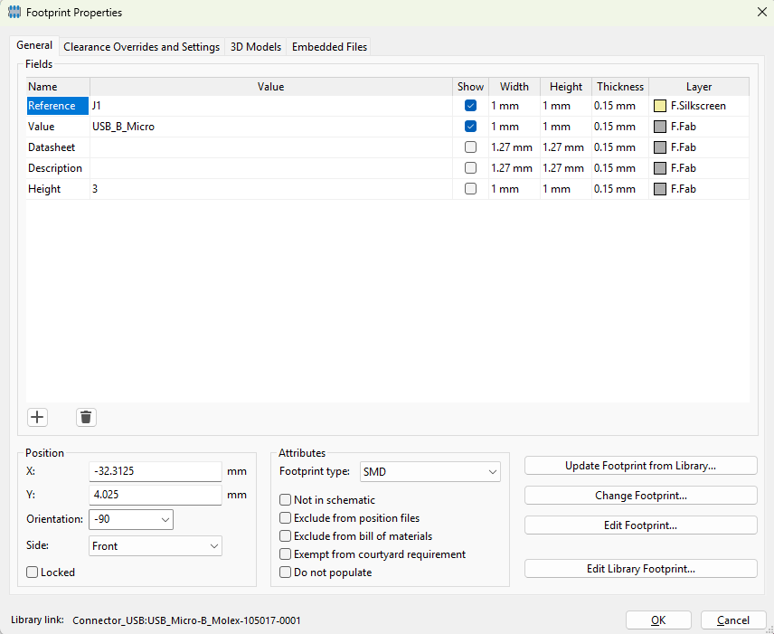
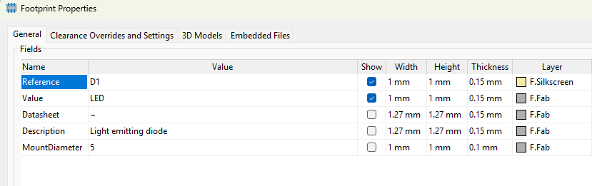
For best results, export your PCB as an STL file so it can be displayed inside the generated enclosure in OpenSCAD.
File → Export → STEP / GLB / BREP / XAO / PLY / STL....pcb.stl 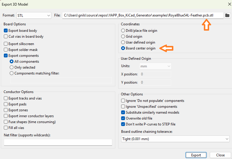
After adding the required footprint properties and optionally exporting the PCB 3D model, open a terminal in the directory containing your .kicad_pcb file and run:
path_to_generateBox inputfile.kicad_pcb [outputfile.scad] [--lightholes]generateBox my_project.kicad_pcb my_project_box.scad| Option | Description |
|---|---|
--lightholes | Generate simple LED holes instead of light tubes |
--noopen | Disable auto open OpenSCAD program |
--help | Display usage information |
--version | Display version information |
Add the required custom properties to your KiCad footprints.
(Optional) Export the PCB as an STL file.
Run the generator on your .kicad_pcb file.
The tool generates:
If OpenSCAD is installed in the default location, it will be launched automatically:
C:\Program Files\OpenSCAD\openscad.exe
Render and export the enclosure in OpenSCAD.
x = 0, Front at positive x (inherited from YAPP_BOX).y cordinate points downThis project builds upon the work of the following open-source tools and libraries:
YAPP_Box
https://github.com/mrWheel/YAPP_Box
Yet Another Parametric Projectbox by Willem Aandewiel, which forms the basis of the generated enclosure code.
KiCad PCB File Parser
https://www.nuget.org/packages/MSDMarkwort.Kicad.Parser.PcbNew
Used for parsing KiCad PCB files and extracting component metadata.
OpenSCAD
https://www.openscad.org
The 3D modeling engine used to render the final enclosure designs.
This project is licensed under the MIT License.
| Qty | Value | Footprint | References |
|---|---|---|---|
| 281 | AUTO_VIA | VIA_MATRIX | V10_10, V10_49, V11_6, V11_10, V11_11, V11_12, V11_13, V11_14, V11_15, V11_16, V11_48, V11_49, V12_12, V12_13, V12_14, V12_15 +265 |
| 10 | 100n | Capacitors_SMD:C_0603_HandSoldering | C2, C3, C4, C5, C6, C13, C16, C17, C19, C20 |
| 3 | 10K | Resistors_SMD:R_0603_HandSoldering | R2, R5, R6 |
| 3 | 2u2 | Capacitors_SMD:C_0603_HandSoldering | C1, C11, C14 |
| 2 | 220n | Capacitors_SMD:C_0603_HandSoldering | C9, C18 |
| 2 | 2n2 | Capacitors_SMD:C_0603_HandSoldering | C7, C8 |
| 2 | 470 | Resistors_SMD:R_0603_HandSoldering | R3, R4 |
| 2 | 47K | myfootprints:TC-33X-2 | RV1, RV2 |
| 1 | 10u | Capacitors_SMD:C_0603_HandSoldering | C12 |
| 1 | 1u | Capacitors_SMD:C_0603_HandSoldering | C15 |
| 1 | 33K | Resistors_SMD:R_0603_HandSoldering | R1 |
| 1 | 470u | Capacitors_Tantalum_SMD:Tantalum_Case-D_EIA-7343-31_Hand | C21 |
| 1 | 47u | Capacitors_SMD:C_0805_HandSoldering | C10 |
| 1 | BTN_1-4 | Terminal_Blocks:TerminalBlock_Pheonix_MPT-2.54mm_4pol | J1 |
| 1 | BTN_5-7 | Terminal_Blocks:TerminalBlock_Pheonix_MPT-2.54mm_3pol | J2 |
| 1 | BTN_8-11 | Terminal_Blocks:TerminalBlock_Pheonix_MPT-2.54mm_4pol | J3 |
| 1 | HIGH | Resistors_SMD:R_0603_HandSoldering | JP1 |
| 1 | LOW | Resistors_SMD:R_0603_HandSoldering | JP2 |
| 1 | MX-503398-1892 | myfootprints:MX-503398-1892 | U4 |
| 1 | PAM8403 | myfootprints:SOP16L | U3 |
| 1 | PCM5100 | Housings_SSOP:TSSOP-20_4.4x6.5mm_Pitch0.65mm | U2 |
| 1 | SPK_OUTL | Pin_Headers:Pin_Header_Straight_1x02 | P2 |
| 1 | SPK_OUTR | Pin_Headers:Pin_Header_Straight_1x02 | P3 |
| 1 | ST-LINK | Pin_Headers:Pin_Header_Straight_1x06_Pitch2.54mm | P1 |
| 1 | STM32F410RBT6 | Housings_QFP:LQFP-64_10x10mm_Pitch0.5mm | U1 |
| 1 | Supply | Pin_Headers:Pin_Header_Straight_1x02_Pitch2.54mm | P4 |
The 323 most common of 329 parts.
gnilsson2/YAPP_Box_KiCad_Generator
Generate Openscad boxes from KiCad PCB files.

gnilsson2/YAPP_Box_KiCad_Generator
Generate Openscad boxes from KiCad PCB files.

gnilsson2/YAPP_Box_KiCad_Generator
Generate Openscad boxes from KiCad PCB files.

gnilsson2/YAPP_Box_KiCad_Generator
Generate Openscad boxes from KiCad PCB files.


polpo/picogus
Emulation of ISA sound cards and CD-ROM on Raspberry Pi Pico (GUS, SB/Adlib, MPU-401, Tandy, CMS, Panasonic CD-ROM) with USB mouse/joystick support


intergalaktik/Extension_Boards_for_Olimex_GateMate
Simple extension boards for Olimex GateMate FPGA Board

saybur/dac-attack
S/PDIF to line-level audio board for use with retro computer device emulators, such as ZuluSCSI and friends.

It measures 39.7 × 50 mm and has 2 copper layers, 1.6 mm thick.
329 parts, built around the STM32F410RBT6, PAM8403 and PCM5100PW. The full list of its parts is on this page, with links to each part's symbol and footprint where PCBKit's library has them.
From the gnilsson2/YAPP_Box_KiCad_Generator repository on GitHub, at the commit this page was made from: the board is TestProject/TestPcbs/sd_wav_pcm5100/sd_wav_pcm5100.kicad_pcb. PCBKit opens the board in the browser, with nothing to install.
Its repository publishes it under the MIT licence: you may reuse it on that licence's terms (keep the author's notice, and for a copyleft licence share your changes alike).