2 layers44.5 × 72.7 mm
OSO SWAT C1-jig
joeycastillo/Sensor-Watch
A board replacement for the classic Casio F-91W wristwatch
28 parts2.1k

 FreezeManny/freezepad
Pro Micro, Choc V1 based Macro/Numpad
Freezepad pcb is an open-source printed circuit board by FreezeManny, from the FreezeManny/freezepad repository on GitHub, published under the GPL-3.0 licence. It is a 2-layer board of 74 × 87 mm with 28 parts on 25 nets, routed with 184 tracks and 6 vias.
It belongs with the keyboards and input boards of this library.
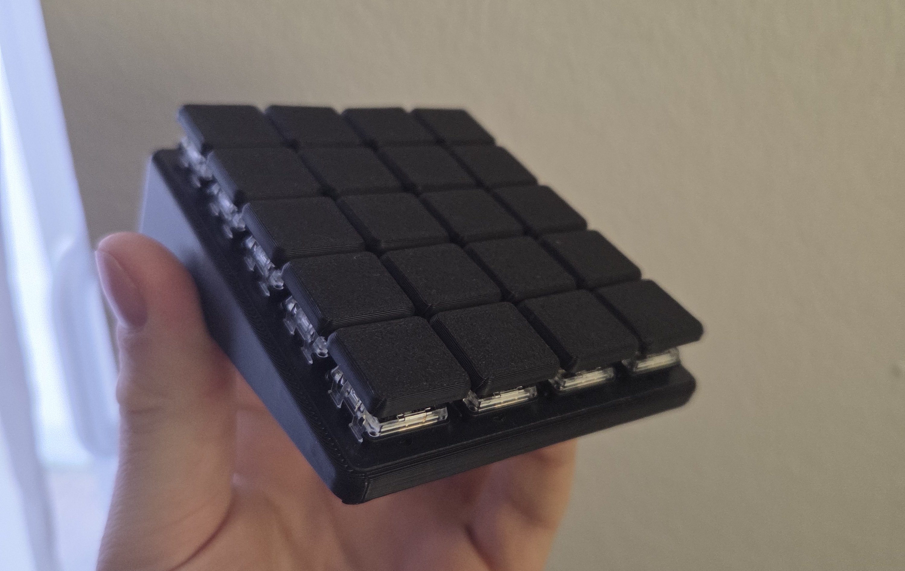
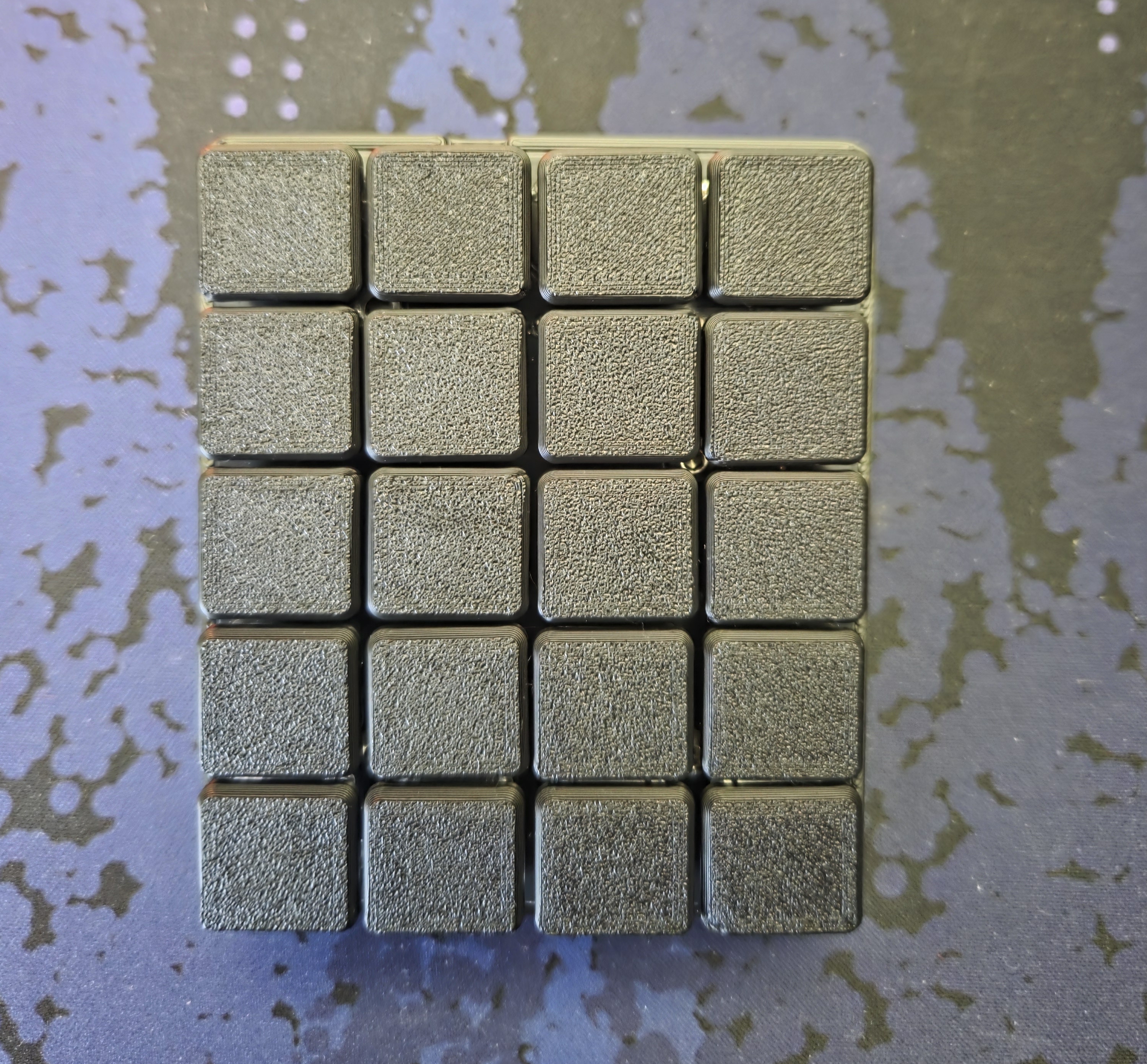
This repository contains all files and configuration for the Freezepad, a custom wireless 20-key (5×4) low-profile macropad built completely from scratch. The goal was to create the smallest possible macropad footprint — achieved by placing the Nice!Nano v2 controller directly below the switches and eliminating diodes entirely. It runs ZMK firmware and is housed in a custom 3D printed case.
| Component | Item | Notes |
|---|---|---|
| PCB | Custom Freezepad PCB | Ordered from JLCPCB. Files in /pcb/. |
| Small Electronics | 1x Push Button 6x2mm, 20x Kailh Choc V1 Hotswap Sockets, 1x Battery Switch | Ordered from AliExpress. |
| Small Case Parts | 3x M3 Heat Insert, 3x M3 Screw | For securing the PCB to the case. |
| Controller | 1x Nice!Nano v2 (or compatible) | Wireless connectivity via Bluetooth. |
| Battery | 1x 102050 LiPo (1000mAh) | Fits in the custom case. |
| Switches | 20x Kailh Choc V1 | e.g., Sunset, Robins. |
| Keycaps | 20x Choc V1 Keycaps | e.g., MBK Blank Choc Keycaps. |
| Case | Custom 3D Printed Case | Files are located in the /case directory. |
The custom PCB was designed using Ergogen. The files are located in the /pcb/ directory.
The Freezepad runs on ZMK Firmware, designed for wireless keyboards and macropads.
/config/ directory.build.yaml)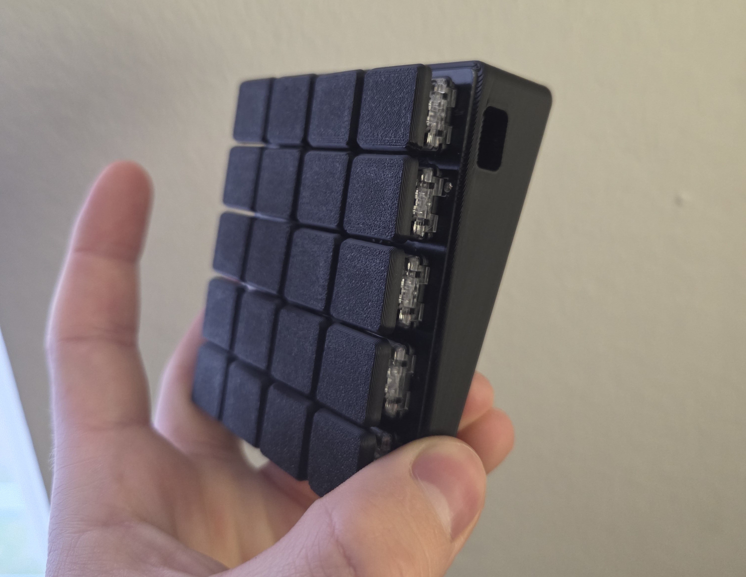
A custom case designed in Fusion360. Source and STEP files are provided in /case.
| Qty | Value | Footprint | References |
|---|---|---|---|
| 20 | PG1350 | S1, S2, S3, S4, S5, S10, S11, S12, S13, S14, S15, S16, S17, S18, S19, S20 +4 | |
| 1 | kbd:ResetSW | B1 | |
| 1 | ceoloide:battery_connector_jst_ph_2 | JST1 | |
| 1 | E73:SPDT_C128955 | T1 | |
| 1 | ProMicro | MCU1 |
The 24 most common of 28 parts.
It measures 74 × 87 mm and has 2 copper layers, 1.6 mm thick.
28 parts. The full list of its parts is on this page, with links to each part's symbol and footprint where PCBKit's library has them.
From the FreezeManny/freezepad repository on GitHub, at the commit this page was made from: the board is pcb/freezepad-pcb.kicad_pcb. PCBKit opens the board in the browser, with nothing to install.
Its repository publishes it under the GPL-3.0 licence: you may reuse it on that licence's terms (keep the author's notice, and for a copyleft licence share your changes alike).
joeycastillo/Sensor-Watch
A board replacement for the classic Casio F-91W wristwatch

TalismanDesign/PocketMage_PDA
An E-Ink PDA device using the ESP32 S3.

rusefi/rusefi
rusefi - GPL internal combustion engine control unit

hackclub/OnBoard
💡 Join 1,000 teenagers and make your first PCB with a $100 grant!

asterics/esp32_mouse_keyboard
ESP32 implementation for HID over GATT Keyboard and Mouse (Bluetooth Low Energy). Including serial API for external modules (similar to Adafruit EZKey HID)


Luos-io/luos_engine
Open-source and real-time orchestrator for cyber-physical-systems, to easily design, test and deploy embedded applications and digital twins.

Chrismettal/EleLab_v2
Cheap DIY lab system for hobbyists and the tinkering folk