2 layers100 × 18.7 mm
Workshop 3
Tessavana/Soft-interfaces-files
Sharing all circuit, PCB, code and design files to be able to replicate EOP soft interfaces
2,819 partsApache-2.0

 FrankBuss/mesh
This project implements a 30x30 node resistor mesh for testing it approximately. The mesh contains 1,740 resistors (870 horizontal + 870 vertical connections), each a 1kΩ 0805 SMD resistor with 0.1% precision.
Mesh is an open-source printed circuit board by FrankBuss, from the FrankBuss/mesh repository on GitHub. It is a 2-layer board of 261.6 × 261.6 mm with 2,821 parts on 961 nets, routed with 3,720 tracks and 0 vias.
A popular question is the resistance between nodes in an infinite grid of resistors, like this:
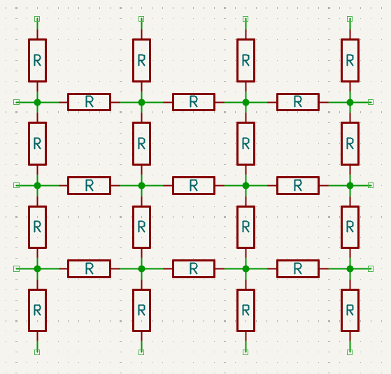
This project implements a 30x30 node resistor mesh for testing it approximately. The mesh contains 1,740 resistors (870 horizontal + 870 vertical connections), each a 1kΩ 0805 SMD resistor with 0.1% precision.
For creating the PCB layout, I used the mesh.py Python script, which automates the placement of the resistors, connections, and vias on each node for easier measurement in the grid pattern, for a KiCAD board, looks like this:
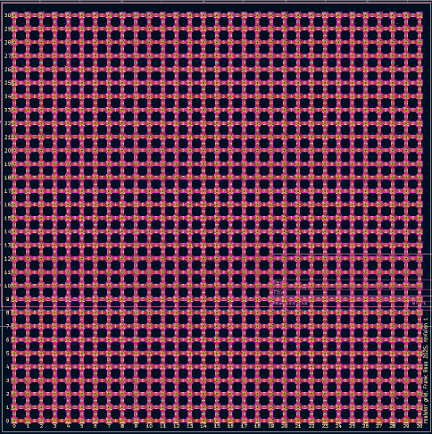
You can download the board here: mesh.kicad_pcb.
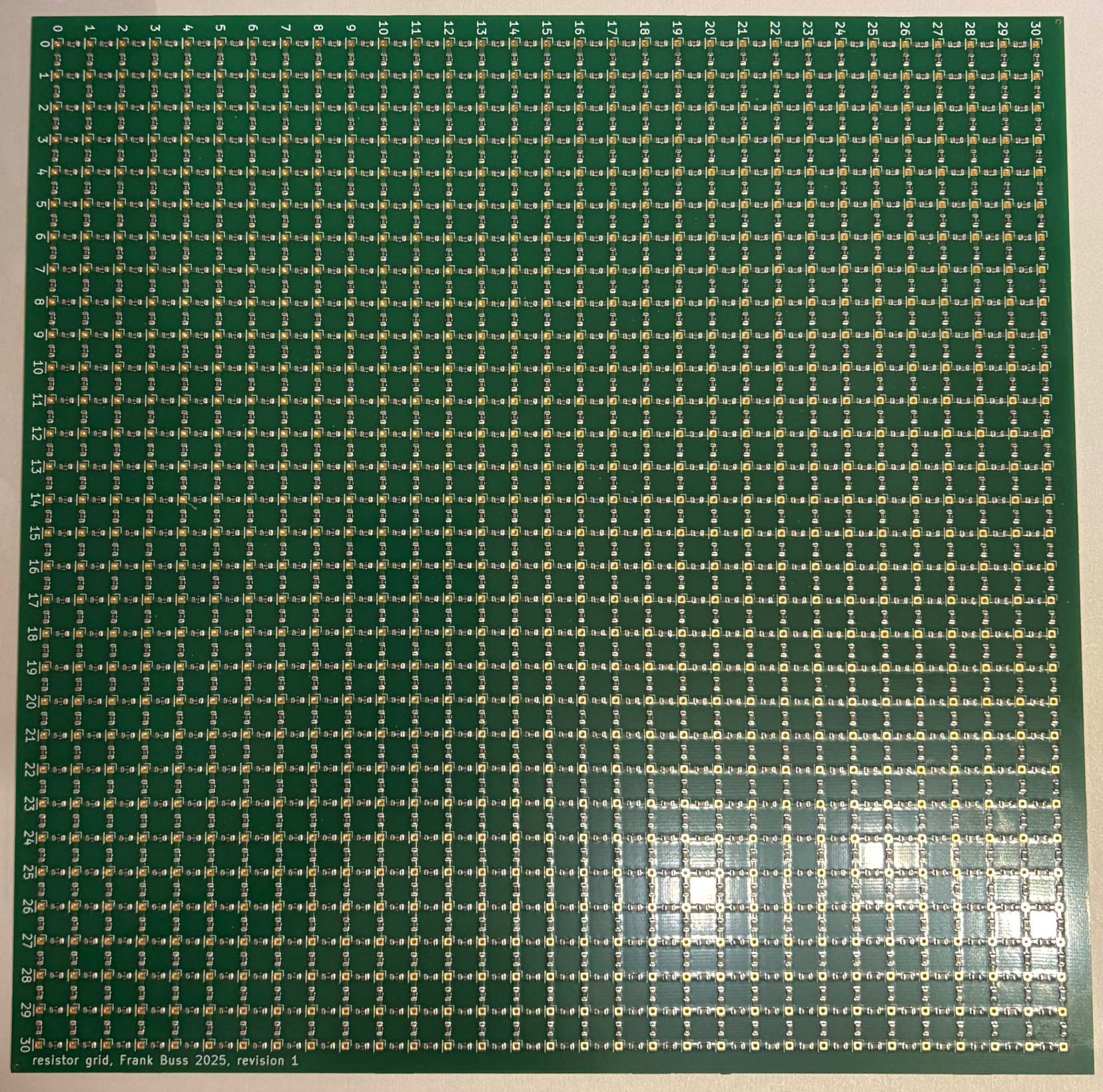
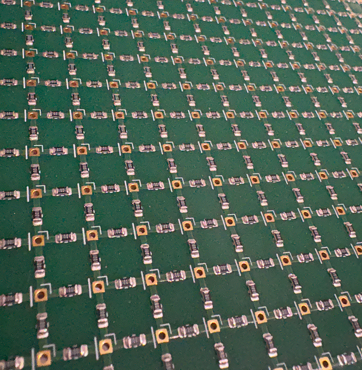
The board was manufactured by JLCPCB, including populating all resistors, using the following production files:
5 boards, 2 of them with populated resistors, did cost $259.99 with shipping.
For an infinite 2D square resistor grid with resistance R per element, the theoretical analysis gives the resistance between nodes separated by (m,n) as:
General formula (equation 9 from the analysis):
R_{(m,n)} = \frac{1}{\pi} \int_0^{\pi} \frac{[1 - e^{i(n\arccos(2-\cos(\alpha)))}] \cos(m\alpha)}{\sin[\arccos(2-\cos(\alpha))]} \, d\alphaThis integral evaluates to specific values:
Adjacent nodes (1,0):
R_{(1,0)} = \frac{1}{2} \cdot R = 500 \text{ Ω}Diagonal nodes (1,1):
R_{(1,1)} = \frac{2}{\pi} \cdot R = 0.63662 \cdot R = 636.62 \text{ Ω}Knight's move (2,1):
R_{(2,1)} = \left(\frac{4}{\pi} - \frac{1}{2}\right) \cdot R = 0.77324 \cdot R = 773.24 \text{ Ω}Since our grid is finite (30x30), edge effects cause small deviations from the infinite grid values. The simulate_grid.py script uses nodal analysis to solve the exact resistance values for the finite grid:
Method: The simulation builds an admittance matrix based on Kirchhoff's current law, injects 1A between two nodes, and solves for all node voltages using sparse matrix methods.
Simulated values for 30x30 grid:
Comparison of measured values with theory:
| Configuration | Measured | Infinite Grid | Finite Grid (30x30) | Error vs Infinite | Error vs Finite |
|---|---|---|---|---|---|
| Adjacent (1,0) | 500.2 Ω | 500.00 Ω | 500.61 Ω | 0.04% | 0.08% |
| Diagonal (1,1) | 640.0 Ω | 636.62 Ω | 637.84 Ω | 0.53% | 0.34% |
| Knight's move (2,1) | 778.0 Ω | 773.24 Ω | 776.29 Ω | 0.62% | 0.22% |
These results demonstrate:
| Qty | Value | Footprint | References |
|---|---|---|---|
| 1860 | R | Resistor_SMD:R_0805_2012Metric_Pad1.20x1.40mm_HandSolder | R1, R10, R100, R101, R1000, R1001, R1002, R1003, R1004, R1005, R1006, R1007, R1008, R1009, R1010, R1011 +1844 |
| 961 | TestPoint | Connector_PinHeader_2.54mm:PinHeader_1x01_P2.54mm_Vertical | TP, TP, TP, TP, TP, TP, TP, TP, TP, TP, TP, TP, TP, TP, TP, TP +945 |
It measures 261.6 × 261.6 mm and has 2 copper layers, 1.6 mm thick.
2,821 parts. The full list of its parts is on this page, with links to each part's symbol and footprint where PCBKit's library has them.
From the FrankBuss/mesh repository on GitHub, at the commit this page was made from: the board is mesh.kicad_pcb and its schematic mesh.kicad_sch. PCBKit opens the board in the browser, with nothing to install.
Its repository states no licence, so its author keeps all rights: ask FrankBuss before reusing the design.
Tessavana/Soft-interfaces-files
Sharing all circuit, PCB, code and design files to be able to replicate EOP soft interfaces

SolderedElectronics/IO-expander-MCP23017-breakout-hardware-design
Hardware design, BOM, gerbers and 3D files for IO-expander-MCP23017-breakout designed by Soldered Electronics.

galopago/misistemote
Misistemote is an Open Source, modular ecosystem that uses pre-made PCB to mix and match your choice of processor board.


embeddedos-org/eCAD-Hardware-Products
Hardware designs + EE docs + Board datasheets of Multiple products

idlehandsdev/black_rabbit
A low poly LED mask made completely out of circuit boards. Second version of a series of high tech face changing masks.


SolderedElectronics/I2C-multiplexer-TCA9548A-breakout-hardware-design
Hardware design, BOM, gerbers and 3D files for I2C-multiplexer-TCA9548A-breakout designed by Soldered Electronics.