4 layers73.5 × 293.4 mm
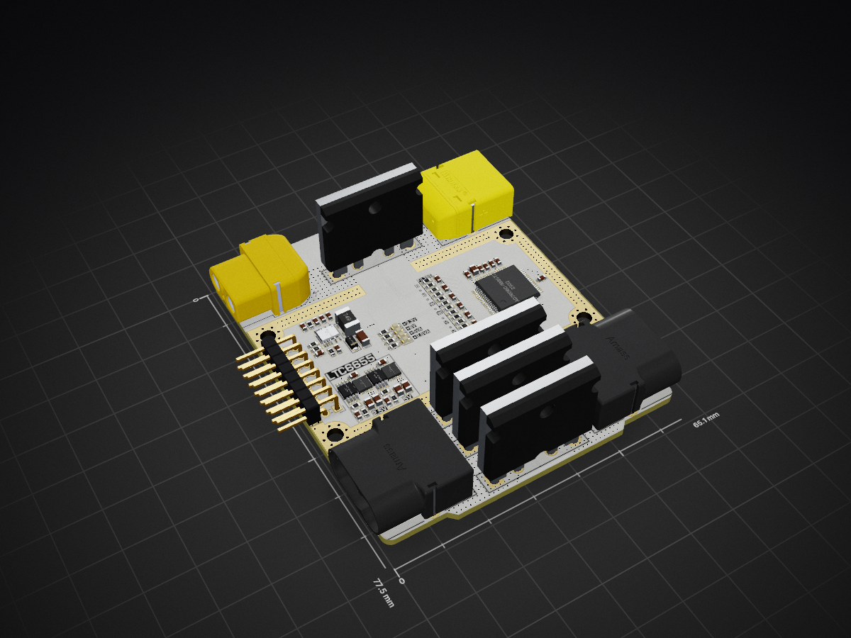
 foukouda/OPEN_PHASE1
OPEN_PHASE: 3-phase inline current and voltage sensing PCB for BLDC drone motors (OPEN THRUST LAB). 1 mΩ shunts + INA241A2 (enhanced PWM rejection), AD7606C-18 18-bit 1 MSPS simultaneous-sampling ADC, LT8362 + LT3045-1 + LTC6655 low-noise analog rails, MR60PW and XT60PW-M connectors. Captures Va/Vb/Vc and Ia/Ib/Ic to compute power and efficiency.
OPEN PHASE is an open-source printed circuit board by foukouda, from the foukouda/OPEN_PHASE repository on GitHub, published under the CERN-OHL-P-2.0 licence. It is a 4-layer board of 65.1 × 77.5 mm with 125 parts on 100 nets, routed with 495 tracks and 1,190 vias.
It is built around the AD7606C-18BSTZ, LT8362EMSE#PBF and LT3045EDD-1#TRPBF, with the LTC6655BHMS8-2.5#PBF, LTC6655BHMS8-5#PBF and PBV-R001-F1-1.0 among its other parts. Its parts include 46 resistors, 39 capacitors, 10 ICs, 5 diodes and 5 connectors. It belongs with the robots and motor control boards of this library.



3-phase inline current and voltage sensing PCB for BLDC drone motors (INA241A2 + AD7606C-18)
Sub-project of OPEN THRUST LAB




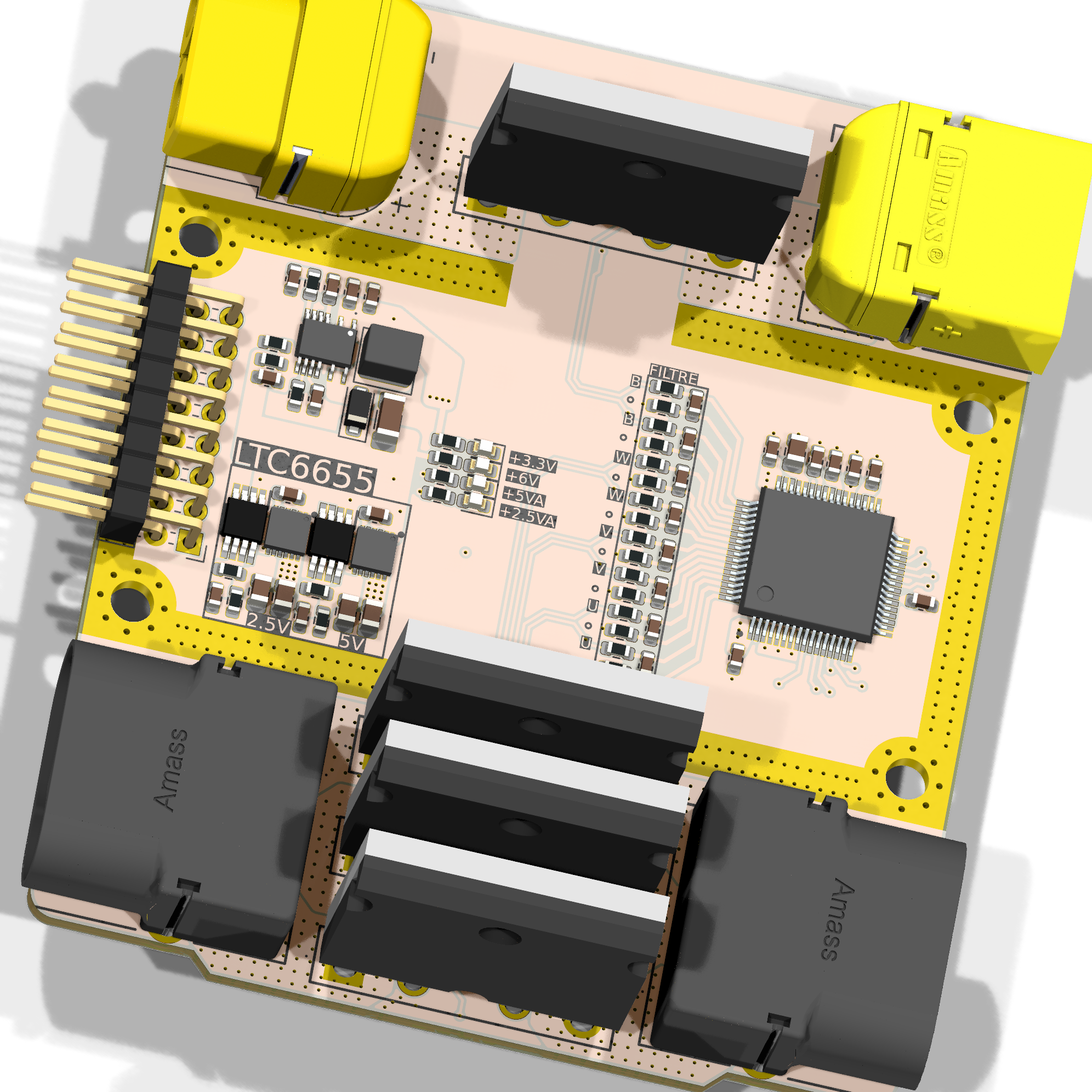
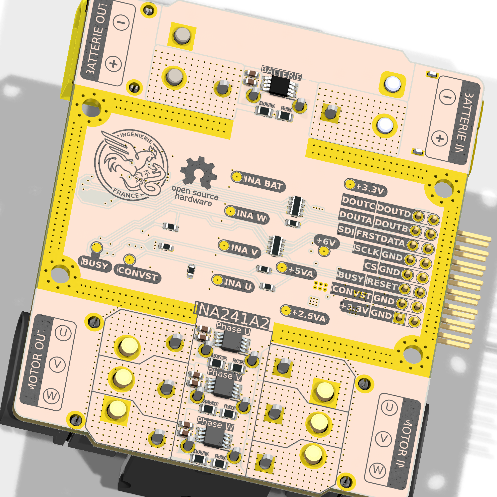
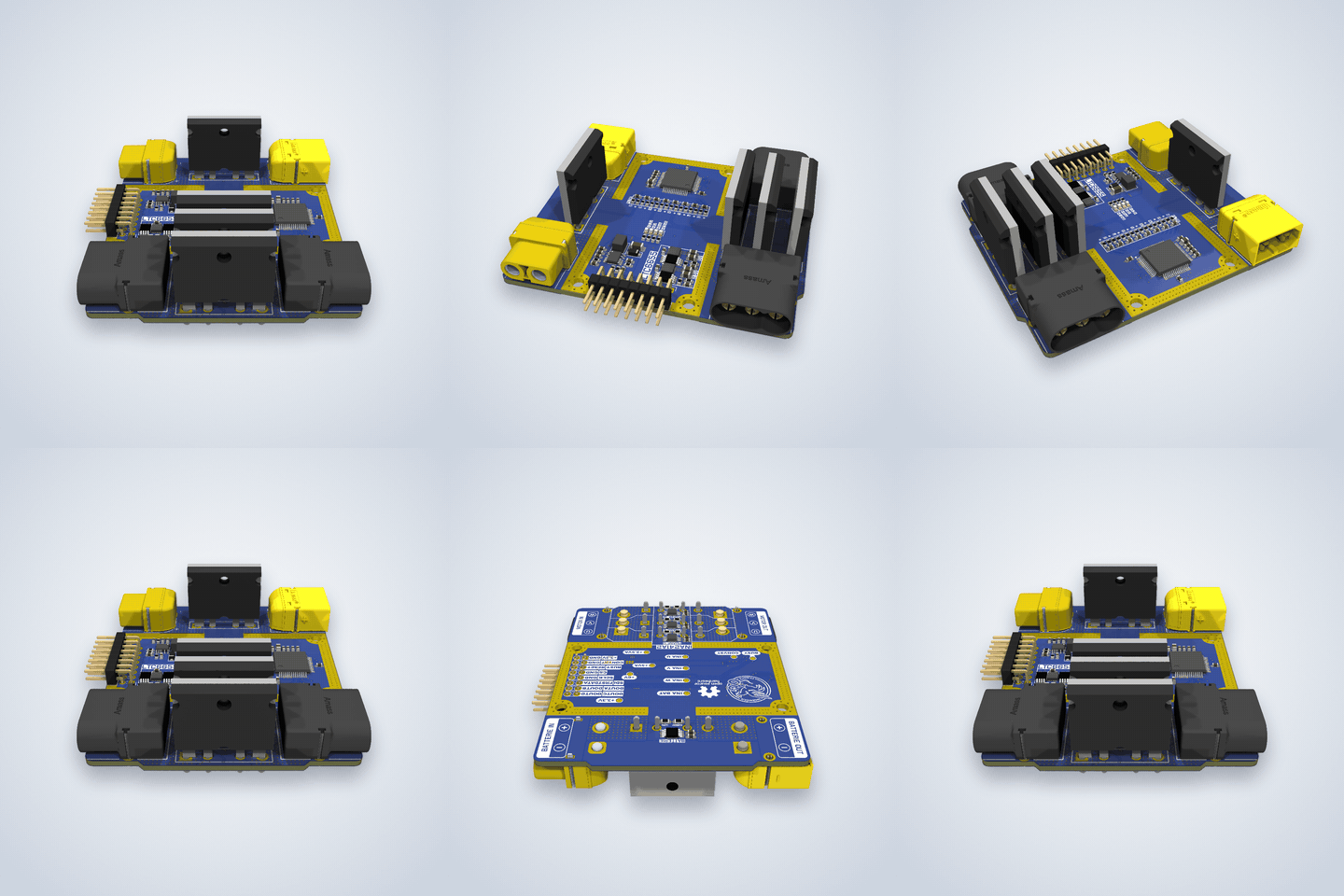
Full-resolution video: Images/OPEN_PHASE.mp4 (KiCad raytracing, kicad-cli pcb render)
OPEN_PHASE is an open-hardware measurement board developed as part of OPEN THRUST LAB, a community-driven project building open-source test benches for drone motor characterization.
The board is inserted between the ESC and a 3-phase BLDC motor (two Amass MR60PW connectors) and between the battery and the ESC (two Amass XT60PW connectors). On each motor phase (U, V, W) and on the battery line (B) it measures:
The eight signals are sampled simultaneously by an Analog Devices AD7606C-18 (8 channels, 18 bits, 1 MSPS), so that power, efficiency and ESC behaviour can be computed from time-aligned Vu/Vv/Vw, Iu/Iv/Iw and the battery voltage and current Vb/Ib.
The board only needs 3.3 V. An LT8362 boost converter (2 MHz) makes 6 V, and two LT3045-1 ultralow-noise LDOs make the analog rails. Each LDO has its SET pin driven by an LTC6655 precision reference, so the LDO works as a low-noise buffer for the reference: +5VA (ADC and amplifier supply) and +2.5VA (ADC reference and amplifier zero-current level).
This project was first published as PhaseSense-8586, after the first version of the design (INA240 + ADS8586S). The schematic now uses the INA241A2 and the AD7606C-18; everything in this README is taken from the current netlist.
This revision is not ready for fabrication. What is in the repository today:
| Area | State |
|---|---|
| Analog front-end (shunts, INA241A2, dividers, input filters) | Drawn and routed |
| AD7606C-18 supply, reference and analog inputs | Drawn and routed |
| AD7606C-18 digital interface (CONVST, BUSY, CS, SCLK, SDI, DOUTA–D, RESET, FRSTDATA) | Drawn: software mode (OS0–2 high), serial (PAR/SER SEL high), external reference (REF SELECT low), to the host connector J4. Not routed on the PCB |
| +3.3V input | J4 pin 1, from the host |
| Power supply (LT8362, LTC6655, LT3045-1) | Drawn; the boost stage is not placed on the PCB (37 unrouted connections) |
| ERC / DRC | 43 ERC and 126 DRC violations, CI runs the PRELIMINARY variant (no ERC/DRC gate) |
See DESIGN REVIEW for the points found while documenting and simulating the design.
| Parameter | Value |
|---|---|
| Input voltage | 3.3 V (LT8362 input range starts at 2.8 V) |
| Boost output — LT8362 | 5.98 V, 2 MHz (RT = 20 kΩ), FBX divider R5/R6 = 1 MΩ / 365 kΩ |
| Analog supply +5VA | 5.000 V — LTC6655-5 (IC7) driving the SET pin of an LT3045-1 (IC8) through R8 = 1 kΩ |
| Reference rail +2.5VA | 2.500 V — LTC6655-2.5 (IC3) driving the SET pin of an LT3045-1 (IC9) through R11 = 1 kΩ |
| Digital supply (AD7606C VDRIVE) | 3.3 V, from the host |
| ADC | AD7606C-18, 8-channel simultaneous sampling, 18 bits, 1 MSPS, external reference on REFIN/REFOUT |
| Current sensing | 4 × PBV-R001 1 mΩ shunt + INA241A2 (20 V/V): 20 mV/A, zero current = 2.5 V |
| Current range | ±35 A continuous on the phases (MR60PW rating) = 2.5 V ± 0.7 V, 30 A on the battery line (XT60PW rating); the amplifier output swing allows about ±115 A |
| Voltage sensing | 4 × divider 40.2 kΩ / 10 kΩ: 0.1992 V/V unloaded, 0.1977 V/V with the AD7606C input impedance |
| Voltage range | 50 V on a ±10 V ADC range (25.2 V for a 6S pack gives 4.98 V) |
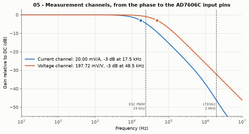
| Current channel bandwidth | 17.5 kHz (phase U: R15 = 33 Ω, R16 = 9.1 kΩ, C25 = 1 nF) |
| Voltage channel bandwidth | 48.5 kHz (phase U: divider + Re1 = 1 kΩ, R19 = 9.1 kΩ, C31 = 180 pF) |
| Phase connectors | 2 × Amass MR60PW (J1 = IN-U/V/W from the ESC, J2 = OUT-U/V/W to the motor), 35 A |
| Battery connectors | 2 × Amass XT60PW (J3 = IN-B from the battery, J5 = OUT-B to the ESC), 30 A |
| AD7606C input | Signal | Source |
|---|---|---|
| V1 | Battery voltage | OUT-B, R32 / R33, Re4, C40, R34 |
| V2 | Battery current | R9 shunt, IC10, R30, C42, R31 |
| V3 | Phase W voltage | OUT-W, R27 / R28, Re3, C34, R29 |
| V4 | Phase W current | R7 shunt, IC6, R25, C33, R26 |
| V5 | Phase V voltage | OUT-V, R22 / R23, Re2, C32, R24 |
| V6 | Phase V current | R4 shunt, IC4, R20, C29, R21 |
| V7 | Phase U voltage | OUT-U, R17 / R18, Re1, C31, R19 |
| V8 | Phase U current | R1 shunt, IC2, R15, C25, R16 |
The four channels are numbered alike: Rn = 33 Ω and Rn+1 = 9.1 kΩ (current filter), Rn+2 / Rn+3 = divider, Rn+4 = 9.1 kΩ (voltage filter), with n = 15 (U), 20 (V), 25 (W), 30 (B). Re1 … Re4 are the 1 kΩ series resistors of the voltage filters.
Current sign: IN+ of each INA241 is on the output side of the shunt (J2 for the phases, J5 for the battery), so a current flowing from J1 to J2, or from J3 to J5, lowers the output: V = 2.5 V − 20 mV/A × I(J1→J2). The voltage is measured on the same output side of the shunt.
Power chain: +3.3 V (host) → LT8362 → +6 V → LTC6655 + LT3045-1 → +5VA / +2.5VA
| Load | Rail | Typical current |
|---|---|---|
| AD7606C-18 AVCC (datasheet: 8.5 mA at 10 kSPS, 45 mA at 1 MSPS) | +5VA | 8.5 – 45 mA |
| 4 × INA241A2 (2.5 mA each) | +5VA | 10 mA |
| 2 × LTC6655 (5 mA each) and 2 × LT3045-1 | +6V | ≈ 13 mA |
| Total on +6V (simulated, 1 MSPS) | +6V | 68 mA |
| AD7606C-18 VDRIVE | +3.3V | < 2 mA |
| Board total (simulated, 1 MSPS) | +3.3V | ≈ 133 mA (0.44 W) |
| Parameter | Value |
|---|---|
| Project name | OPEN_PHASE |
| Board name | PHASETRACKER |
| Parent project | OPEN THRUST LAB |
| CAD tool | KiCad 10 |
| Automation tooling | KiBot + GitHub Actions |
| Hardware licence | CERN-OHL-P v2 |
| Dimensions | 65.05 × 77.5 mm |
| Stackup | 4 layers, 1.66 mm, 70 µm outer copper, ENIG |
| Mounting holes | 4 × M3, connected to GND |
Five functional hierarchical sheets (under Project Architecture), plus the documentation sheets (Block Diagram, Power - Sequencing, Revision History):
| Sheet (file) | Description |
|---|---|
AD7606C-18_ADC (AD7606C-18 - ADC.kicad_sch) | AD7606C-18 (IC1). AVCC = +5VA (C20, C35, C38), VDRIVE = +3.3V (C21), REFIN/REFOUT = +2.5VA (C41), REFCAPA/REFCAPB joined on C39 (10 µF), REGCAP pins on C36 / C37 (1 µF each). The eight analog input pairs come from the INA241 sheet through global labels. |
INA241_Phase_Sense (INA241 - Phase Sensing.kicad_sch) | Four identical channels: phases U, V, W and the battery line B. Shunt R1 / R4 / R7 / R9 with Kelvin connection to IC2 / IC4 / IC6 / IC10 (INA241A2, VS = +5VA, REF1 = REF2 = +2.5VA), output filter 33 Ω + 1 nF. Voltage divider 40.2 kΩ / 10 kΩ, 1 kΩ + 180 pF. 9.1 kΩ return resistor on every negative ADC input. |
Connectors (Connectors.kicad_sch) | J1 and J2, Amass MR60PW: pins 1–3 = phases, mounting pins 4–5 = GND. J3 (XT60PW-F) and J5 (XT60PW-M): pin 2 = battery line, through the shunt R9; pin 1 not connected; mounting pins = GND. J4, 2 × 8 pin header 2.54 mm (horizontal, for Dupont wires) to the host: pin 1 = +3.3V, pins 2, 4, 8, 10 = GND, then CONVST (3), BUSY (5), RESET (6), CS (7), SCLK (9), SDI (11), FRSTDATA (12), DOUTA–D (13–16). |
Holes, Fiducials (Holes - Fiducials.kicad_sch) | Four M3 mounting holes H1–H4 connected to GND. |
Power_Supply (Power Supply - Analog Rails.kicad_sch) | LT8362 boost (IC5, L1 = 2.2 µH, D2 = PMEG2020EH, 2 MHz, pulse-skipping, soft-start C24 = 10 nF). LTC6655-5 (IC7) and LTC6655-2.5 (IC3) references, each driving the SET pin of an LT3045-1 (IC8 / IC9) through 1 kΩ with 10 µF on SET. PGFB tied to IN (no Power-Good, no fast start-up), ILIM to GND, VIOC open. |
Points found while checking the documentation against the netlist and the datasheets, and while simulating the design. Unless marked Fixed, none of them has been changed in the schematic: they are design decisions to take.
Two findings on the +2.5VA rail have been fixed.
IC3 was an LTC6655LN-2.5 wired like the standard part, with pin 6 tied to pin 7. On the LN version pin 6 is NR (noise reduction, to be decoupled to ground), not VOUT_S. IC3 is now a standard LTC6655-2.5 on the same footprint, for which this wiring is correct. The LTspice model of the LN part does not model the NR pin, so it could not show what the old connection did.
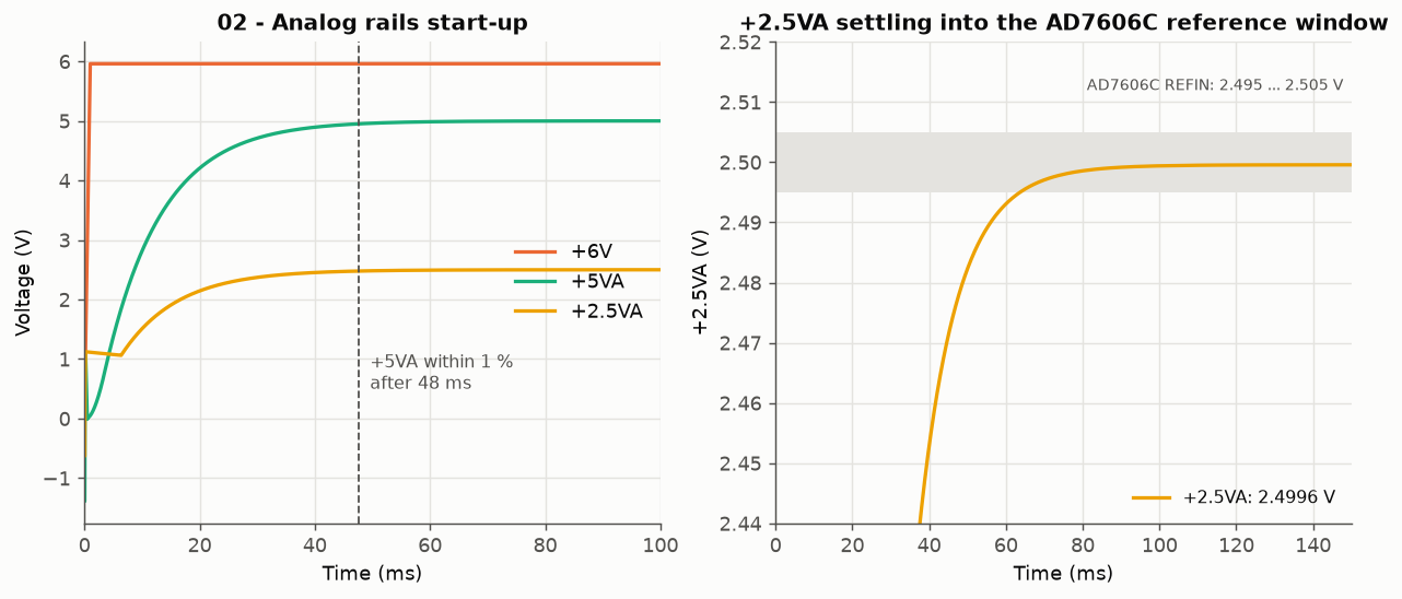
R12, on the SET pin of IC9, was 49.9 kΩ. The LT3045-1 sources 100 µA from SET, so the pin wanted 4.99 V against the 2.5 V reference and +2.5VA settled at 2.549 V, outside the 2.495 – 2.505 V reference window of the AD7606C. R12 is now 24.9 kΩ (100 µA × 24.9 kΩ = 2.49 V): +2.5VA settles at 2.4996 V.
| # | Finding | Evidence | Suggested action |
|---|---|---|---|
| 1 | The AD7606C-18 has no digital interface and the board has no +3.3V input. CONVST, BUSY, CS, RD/SCLK, DOUTA–D, FRSTDATA, RESET, OS0–2, RANGE, PAR/SER SEL, STBY, WR and REF SELECT are open. | Netlist: 32 unconnected-(IC1-…) nets; J1 / J2 and J3 / J5 only carry the phases, the battery line and GND. | Fixed: host connector J4 added, mode pins strapped (software mode, serial, REF SELECT low). |
| 2 | AD7606C-18 pins left open that the datasheet asks to connect: AGND pin 26 and REFGND pin 46 ("All six of the AGND pins must connect to the AGND plane"). | Netlist: unconnected-(IC1-AGND_2-Pad26), …REFGND_2-Pad46. | Fixed: both on GND. |
| 3 | INA241A2 pin 4 (NC) is open on IC2, IC4, IC6 and IC10. The datasheet pin table says: "NC — Reserved. Connect to ground." | Netlist: unconnected-(IC2-NC-Pad4) and the same for IC4, IC6, IC10. | Connect pin 4 to GND. |
| 4 | The INA241A2 gain is 20 V/V. The schematic note listed the INA240 gains (A2 = 50 V/V). With 1 mΩ the scale is 20 mV/A: 35 A only uses ±0.7 V of the ±2.5 V available. | TI datasheet SBOSA30D: A1 = 10, A2 = 20, A3 = 50, A4 = 100, A5 = 200 V/V. The note is corrected in the schematic. | Keep 20 V/V (±115 A range) or fit an INA241A3 (50 V/V, ±46 A) for more resolution. |
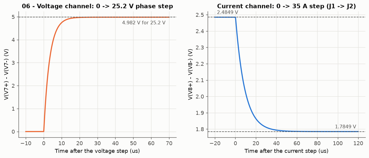
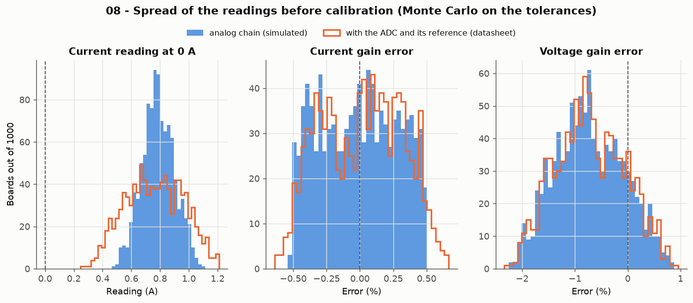
| 5 | Current channels: the 9.1 kΩ return resistor creates a 15 mV offset. The AD7606C inputs are 1.2 MΩ to an internal 2 V node. On the voltage channels both inputs see about 9 kΩ, so the two bias drops cancel (−0.15 mV). On the current channels the positive input sees 33 Ω and the negative one 9.1 kΩ: V− sits at +15 mV. | Simulation 06: 2.4849 V at zero current instead of 2.5000 V, which reads as +0.75 A. | Constant offset: remove it with a zero-current calibration. Do not shrink R16 / R21 / R26 / R31 without recomputing the filter: the capacitor is differential, so they set the 17.5 kHz corner. |
| 6 | Voltage channels: −0.75 % gain error from the 9 kΩ source impedance into the 1.2 MΩ input (−0.9 % at the 1 MΩ minimum). | Simulation 05: 0.1977 V/V instead of 0.1992 V/V. | Calibrate, or use the AD7606C per-channel gain register (software mode, 9 kΩ). |
| 7 | PCB not finished: IC5, L1 and the boost passives are outside the board outline, C16 has no schematic symbol, C14 / C15 / C39 use a 4-pin capacitor symbol on a 2-pad footprint. | DRC: 37 unconnected items, 20 schematic parity warnings. | Place and route the boost stage; align symbol and footprint of the 4-terminal capacitors. |
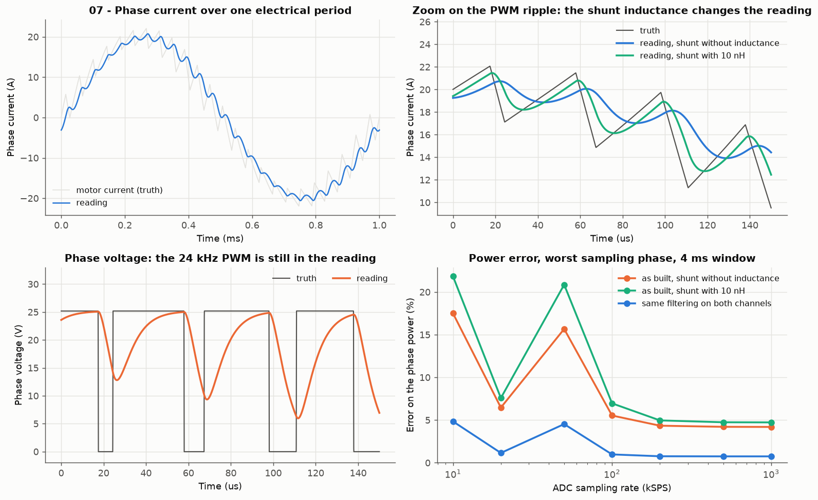
| 8 | The delay between the current and voltage readings is not known before a board exists. The current channel has a 17.5 kHz filter and the voltage channel a 48.5 kHz one, and the inductance of the shunt (datasheet: below 10 nH) acts against the filter of the current channel. Under PWM, a phase difference between the two readings at the switching frequency turns reactive power into measured power. | Simulation 07, phase power after DC calibration: −4.2 % with 0 nH, +0.3 % with 5 nH, +4.7 % with 10 nH. With a time shift of the current calibrated at the electrical frequency: within ±1.5 %. | Measure the phase between the two channels on the first board, then choose C31 / C32 / C34 or correct the delay in the firmware. |
| 9 | AD7606C-18 VDRIVE is above AVCC + 0.3 V at power-up. VDRIVE = +3.3V comes from the host and is there at once, while AVCC = +5VA (boost, then LTC6655 + LT3045-1) only passes 3.0 V after about 10 ms. | Datasheet Rev. B, Table 6: "VDRIVE to AGND −0.3 V to AVCC + 0.3 V". | Low-Vf Schottky from +3.3V (anode) to +5VA (cathode), reverse-biased in operation, or VDRIVE from a 3.3 V LDO on +5VA with the host keeping its pins low until the rails are up. |
The power chain and the two measurement channels are simulated with LTspice 26 in Simulation/LTspice/. Every component value comes from the KiCad netlist and keeps its reference designator, so the simulation schematics can be read side by side with the KiCad sheets.
| File | Analysis | What it checks |
|---|---|---|
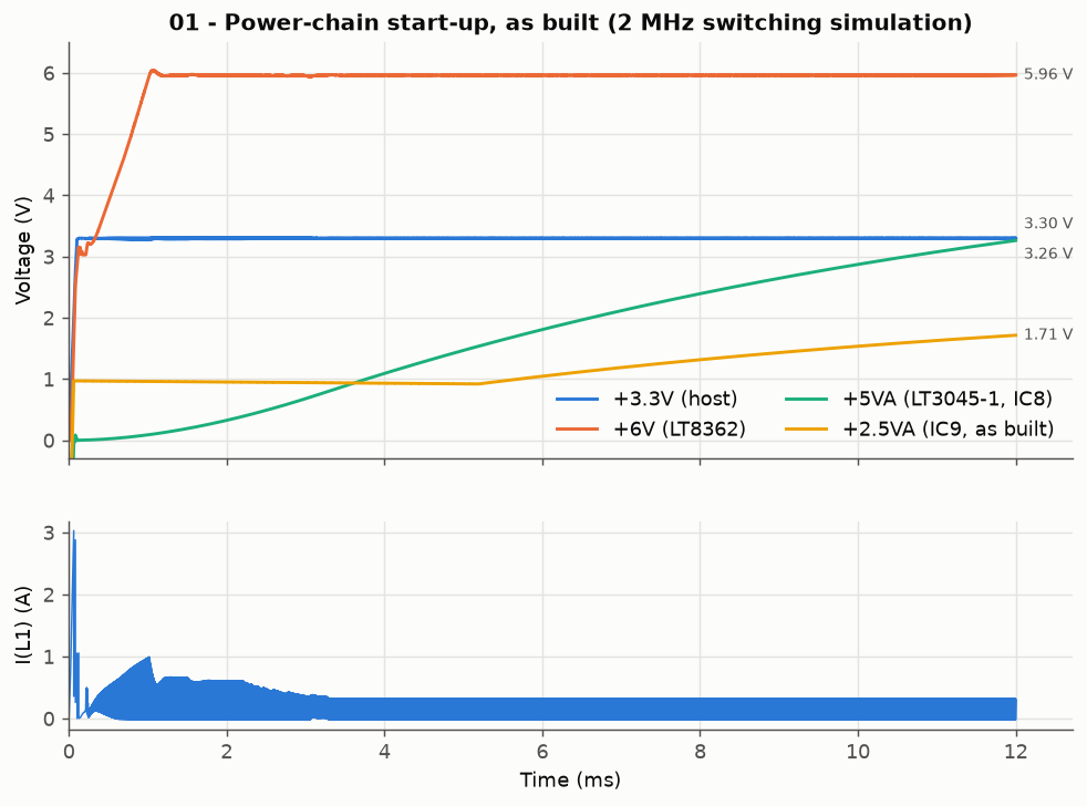
01_Power_Chain_Startup.asc | .tran 12 ms, switching | +3.3V → LT8362 → +6V → LT3045-1 soft-start, inrush and inductor current (board as built) |
02_Analog_Rails_Startup.asc | .tran 150 ms | Settling and accuracy of +5VA and +2.5VA |
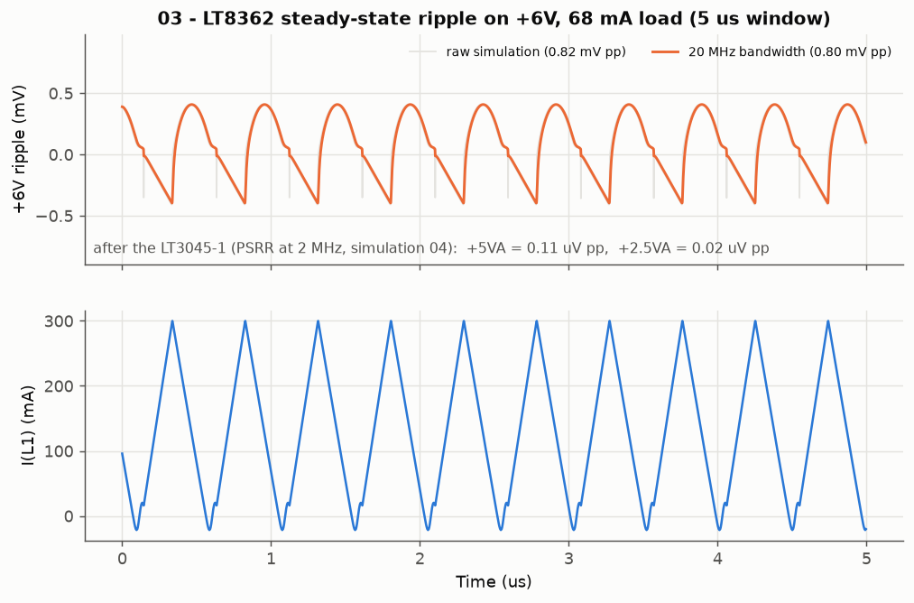
03_Boost_Ripple.asc | .tran 6 ms, switching | LT8362 steady-state ripple on +6V with the simulated load of both rails |
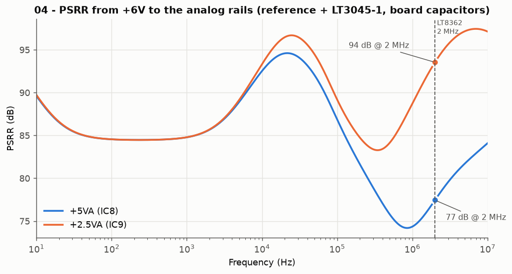
04_Analog_Rails_PSRR.asc | .ac 10 Hz – 10 MHz | Rejection from +6V to +5VA and +2.5VA (reference + LDO, board capacitors) |
05_Measurement_Channels_AC.asc | .ac 10 Hz – 10 MHz | Gain and bandwidth of the current and voltage channels, down to the ADC pins |
06_Measurement_Channels_Step.asc | .tran 600 µs | DC transfer, offsets and settling for a 25.2 V and a 35 A step |
07_Measurement_Quality_Waveforms.asc | .tran 8 ms, 3 runs | ESC PWM voltage and motor current through both channels of phase U, battery voltage and current through the battery channels: readings against the truth, for a shunt inductance of 0, 5 and 10 nH |
08_Measurement_Quality_Tolerances.asc | .dc, 1000 runs | Monte Carlo on the tolerances: spread of offset and gain before calibration |
Models
INA241A2_behav.sub / .asy is a behavioral model written for this project from the datasheet (SBOSA30D): gain 20 V/V around (REF1 + REF2) / 2, 1.1 MHz bandwidth, 8 V/µs slew rate, output swing, 2.5 mA supply current, 35 µA input bias. Gain and input offset are parameters, nominal except in simulation 08. It does not model noise, CMRR or the 1 µs output hold of the enhanced PWM rejection.Results
| Quantity | Simulated | Notes |
|---|---|---|
| +6V output (LT8362) | 5.96 V | 1.6 V × (1 + 1 MΩ / 365 kΩ) = 5.98 V |
| +6V reaches 90 % | 0.88 ms | 5.9 V after 1.0 ms, 6.04 V overshoot |
| Inrush in L1 / D2 when +3.3V is applied | 3.0 A peak | the 31 µF on +6V charge to VIN through L1 and D2; depends on the rise time of the host rail (100 µs assumed) |
| Peak inductor current during soft-start / steady state | 0.99 A / 0.30 A | L1 (WE-MAPI 4030) loses 10 % at 4.6 A, LT8362 switch limit 2 A min / 3.1 A max |
| +6V ripple, 20 MHz bandwidth | 0.81 mV pp | discontinuous conduction, 68 mA load |
| Current drawn from +3.3V | 133 mA | AD7606C at 1 MSPS |
| +5VA | 4.9998 V | reference 5.0000 V; 100 µA × R14 = 4.99 V, almost no current in R8 |
| +5VA within 1 % / 0.1 % | 48 ms / 71 ms | τ = (R8 ∥ R14) × C13 = 9.8 ms; PGFB = IN disables the LT3045-1 fast start-up |
| +2.5VA | 2.4996 V | reference 2.5000 V; 100 µA × R12 = 2.49 V, almost no current in R11; inside the 2.495 – 2.505 V window of the AD7606C |
| PSRR +6V → +5VA | 85 dB at 1 kHz, 77 dB at 2 MHz | ideal layout |
| PSRR +6V → +2.5VA | 85 dB at 1 kHz, 94 dB at 2 MHz | ideal layout |
| Boost ripple left on +5VA / +2.5VA | 0.11 µV pp / 0.02 µV pp | +6V ripple × PSRR at 2 MHz |
| Current channel gain | 20.00 mV/A | 1 mΩ × 20 V/V |
| Current channel −3 dB | 17.5 kHz | −4.6 dB at 24 kHz, −46 dB at 2 MHz |
| Current channel at 0 A / 35 A (J1→J2) | 2.4849 V / 1.7849 V | 15 mV offset from the ADC input bias in R16 |
| Current channel 1 % settling | 42 µs | |
| Voltage channel gain | 0.1977 V/V | 25.2 V reads 4.982 V |
| Voltage channel −3 dB | 48.5 kHz | −0.95 dB at 24 kHz, −32 dB at 2 MHz |
| Voltage channel 1 % settling | 15 µs |
Re-run the simulations (Windows, LTspice installed in the default location):
cd Simulation/LTspice
python run_simulations.py            # runs LTspice in batch mode, redraws Images/Simulation/*.png, results.md and measurement_quality.md
python run_simulations.py --no-run   # only redraw from the existing .raw files
python generate_asc.py               # rebuilds the .asc files (overwrites hand edits)
Or open any .asc in LTspice and press Run. Simulation 01 switches at 2 MHz for 12 ms and takes about 7 minutes; 03 takes about 2 minutes.
The simulations validate the design intent (regulation, sequencing, filtering). They do not replace bench measurements: layout parasitics, capacitor DC-bias derating and the real PWM edges on the phases will change the figures. The steady-state ripple is simulated on the boost alone because the encrypted LDO and reference models cannot be started from a preset operating point; what is left on the analog rails is computed from the simulated PSRR.
Simulations 07 and 08 estimate how good the measurements will be before a board is built. run_simulations.py compares the readings with the simulated truth, adds what the datasheets say about the parts that are not simulated, and writes the full report to Simulation/LTspice/measurement_quality.md.
How far a reading is from the truth (one reading of a steady value)
| True value | No calibration | Zero taken before the run | Zero and gain calibrated |
|---|---|---|---|
| 5 A | reads 5.41 … 6.12 A | ±0.03 A (±0.5 %) | ±0.008 A (±0.16 %) |
| 10 A | reads 10.41 … 11.13 A | ±0.05 A (±0.5 %) | ±0.017 A (±0.17 %) |
| 20 A | reads 20.39 … 21.13 A | ±0.10 A (±0.5 %) | ±0.041 A (±0.21 %) |
| 35 A | reads 35.35 … 36.16 A | ±0.18 A (±0.5 %) | ±0.105 A (±0.30 %) |
| 12 V | reads 11.76 … 12.07 V | as without calibration | ±0.04 V (±0.33 %) |
| 25.2 V | reads 24.71 … 25.33 V | as without calibration | ±0.08 V (±0.33 %) |
| 50 V | reads 49.05 … 50.27 V | as without calibration | ±0.17 V (±0.33 %) |
Under PWM (simulation 07: 25.2 V battery, 24 kHz PWM, motor phase of 30 µH / 50 mΩ, 20 A peak at 1 kHz, 90 W in the phase)
| Question | Prediction | Comment |
|---|---|---|
| RMS current | −0.4 … −1.0 % | Part of the PWM ripple is filtered: 41 … 75 % of it is left in the reading |
| Mean phase voltage | 0.0 % after calibration | The RMS reads 14 % low because the filters round the PWM edges: use the mean or the fundamental |
| Phase power after DC calibration | −4.2 … +4.7 % | Depends on the inductance of the shunt, between 0 and the 10 nH of its datasheet, see DESIGN REVIEW 8 |
| Phase power once the delay between the channels is calibrated | within ±1.5 % | Time shift of the current measured at the electrical frequency |
| Sampling rate | ≥ 200 kSPS | Below, the PWM aliases into the power: up to 22 % over a 4 ms window |
| Power from the battery | within 0.2 % after DC calibration | Battery voltage and current are almost steady: the delay between the two channels does not matter, from 10 kSPS |
Shunt R1 / R4 / R7 / R9 (PBV-R001-F1-0.5, Isabellenhütte datasheet): tolerance ±0.5 %, temperature coefficient below 75 ppm/K, thermal resistance below 15 K/W (1.2 W and +18 K at 35 A, for 3 W allowed), inductance below 10 nH, thermal EMF below 2 µV/K (2 mA of offset per kelvin of difference between the two sense terminals). The other resistors have no part number in the schematic: 1 % and 100 ppm/K are assumed for them.
Method
Not covered: the common-mode rejection of the INA241A2 and its 1 µs output hold at each PWM edge (behavioural model), the layout, and the other two phases (the waveform is a single-phase equivalent). The PWM figures are for this test waveform; change the
.paramline of simulation 07 for another motor or another PWM frequency.
After 3.3 V is applied (values from the LTspice simulations):
| Stage | Duration | Indicator |
|---|---|---|
| Output capacitors charge to VIN through L1 / D2 | < 0.2 ms | +6V ≈ 3 V |
| LT8362 soft-start (C24 = 10 nF) | +6V at 90 % after 0.9 ms, 5.9 V after 1.0 ms | +6V = 5.96 V |
| LTC6655 references charge their 10 µF and the SET capacitors | 93 % after 3 ms | REF5 → 5 V |
| LT3045-1 outputs follow the SET pins (τ = 9.8 ms) | 1 % after 48 ms, 0.1 % after 71 ms | +5VA, +2.5VA |
| Minimum delay before the first conversion | ≥ 100 ms | rails settled |
The LT3045-1 Power-Good outputs are not used (PGFB tied to IN), so there is no hardware "rails ready" signal: use the delay.
lib/ and referenced relative to the project (KIPRJMOD, project-local sym-lib-table / fp-lib-table)./kibot_launch.sh # default configuration
./kibot_launch.sh -v CHECKED # specific variant| Variant | Outputs | ERC/DRC | Typical use |
|---|---|---|---|
DRAFT | Schematic only | — | Early design work |
PRELIMINARY | Schematic + PCB | — | Layout iterations (current CI setting) |
CHECKED | Full | ✓ enforced | Design review |
RELEASED | Full | ✓ enforced | Tagged version releases |
| Content | Description |
|---|---|
| Schematic sources | KiCad hierarchical schematic, 10 sheets |
| PCB layout | KiCad 4-layer PCB |
| Libraries | lib/ — every symbol, footprint and 3D model used on the board |
| Manufacturing, validation, 3D exports | Generated by the CI (KiBot) |
| Documentation sheets | Block diagram, architecture, power sequencing, revision history |
| CI resources | GitHub Actions workflow, KiBot YAML configuration |
| Simulation | LTspice simulations of the power chain and the measurement channels, predicted measurement quality |
.
├─ Computations       # Design notes and calculations
├─ HTML               # Generated HTML pages
├─ Images             # Pictures, renders
│  └─ Simulation      # Figures drawn by Simulation/LTspice/run_simulations.py
│
├─ kibot_resources    # External resources used by KiBot
│  ├─ colors          # Color themes for KiCad outputs
│  ├─ fonts           # Fonts used in generated documents
│  ├─ scripts         # Helper scripts used with KiBot
│  └─ templates       # Templates for KiBot reports (this README: readme.txt)
│
├─ kibot_yaml         # KiBot YAML configuration files
├─ KiRI               # KiRI PCB diff viewer files
│
├─ lib                # Project libraries (self-contained)
│  ├─ lib_sym         # OPEN_PHASE.kicad_sym — every symbol used
│  ├─ lib_fp          # OPEN_PHASE.pretty — every footprint used
│  └─ 3d_models       # STEP models referenced by the footprints
│
├─ Logos              # Project logos
│
├─ Manufacturing
│ ├─ Assembly # BoM, position files, assembly notesThis project uses a reproducible hardware workflow based on KiCad 10, KiBot and GitHub Actions.
The CI pipeline (.github/workflows/ci.yaml) runs KiBot on every push to dev or main and commits the generated outputs back ("Update Outputs" commits). Always git pull after the CI has run, before editing the project again, otherwise the regenerated files (.kicad_pro, BoM, netlist, README…) will conflict.
ℹ️
README.mdis generated by KiBot fromkibot_resources/templates/readme.txt. Edit the template, notREADME.md, or your changes will be overwritten by the next CI run.
Branch convention: dev is the development branch; main only receives merges from dev and carries the release tags.
Project metadata (project name, board name, company, designer, logo, repository URL) is defined once in kibot_yaml/kibot_main.yaml (definitions: section) and propagated to title blocks, documents and this README.
Release a new hardware revision:
dev, fill the [Unreleased] section of CHANGELOG.md.kibot_variant to CHECKED in ci.yaml once ERC and DRC are clean.dev into main: git checkout main && git pull && git merge dev && git pushv prefix): git tag 1.0.0 && git push origin 1.0.0dev: git checkout dev && git merge mainSee CHANGELOG.md (Keep a Changelog format, semantic versioning).
The hardware design files in this repository are released under the CERN Open Hardware Licence Version 2 – Permissive (CERN-OHL-P v2). See LICENSE for the full licence text.
Copyright 2026 Dimitry Siebert, OPEN THRUST LAB. Source location: https://github.com/foukouda/OPEN_PHASE.
Under CERN-OHL-P v2:
The KiBot configuration and CI workflow come from the KDT_Hierarchical_KiBot template by Nguyen Vincent (MIT licence).
For more on CERN-OHL licences: cern-ohl.web.cern.ch
| Qty | Value | Footprint | References |
|---|---|---|---|
| 10 | TestPoint | OPEN_PHASE:TestPoint_Pad_D1.5mm | TP3, TP4, TP5, TP6, TP9, TP10, TP11, TP12, TP15, TP16 |
| 8 | 33Ω | OPEN_PHASE:R_0603_1608Metric | R15, R20, R25, R30, R35, R36, R37, R38 |
| 8 | 9.1kΩ | OPEN_PHASE:R_0603_1608Metric | R16, R19, R21, R24, R26, R29, R31, R34 |
| 6 | 100nF | OPEN_PHASE:C_0603_1608Metric | C20, C21, C23, C35, C38, C41 |
| 6 | 1kΩ | OPEN_PHASE:R_0603_1608Metric | R8, R11, Re1, Re2, Re3, Re4 |
| 5 | 10µF | OPEN_PHASE:C_0805_2012Metric | C13, C14, C15, C19, C39 |
| 5 | 1µF | OPEN_PHASE:C_0603_1608Metric | C5, C10, C16, C18, C27 |
| 4 | 0.1µF | OPEN_PHASE:C_0603_1608Metric | C1, C2, C3, C17 |
| 4 | 10kΩ | OPEN_PHASE:R_0805_2012Metric | R18, R23, R28, R33 |
| 4 | 180 pF C0G/NP0, 50 V, 0603 | OPEN_PHASE:C_0603_1608Metric | C31, C32, C34, C40 |
| 4 | 1nF C0G | OPEN_PHASE:C_0603_1608Metric | C25, C29, C33, C42 |
| 4 | 40.2kΩ | OPEN_PHASE:R_0805_2012Metric | R17, R22, R27, R32 |
| 4 | INA241A2IDGKR | OPEN_PHASE:SOP65P490X110-8N | IC2, IC4, IC6, IC10 |
| 4 | LED | LED_SMD:LED_0603_1608Metric | D1, D3, D4, D5 |
| 4 | MountingHole_Pad | OPEN_PHASE:MountingHole_3.2mm_M3_Pad_Via | H1, H2, H3, H4 |
| 4 | PBV-R001-F1-1.0 | OPEN_PHASE:PBVR001F110 | R1, R4, R7, R9 |
| 3 | 100kΩ | OPEN_PHASE:R_0603_1608Metric | R42, R43, R44 |
| 3 | 100Ω | OPEN_PHASE:R_0603_1608Metric | R39, R40, R41 |
| 3 | 4.7µF | OPEN_PHASE:C_0603_1608Metric | C9, C11, C22 |
| 2 | 10µF | OPEN_PHASE:C_0603_1608Metric | C8, C12 |
| 2 | 1uF | OPEN_PHASE:C_0603_1608Metric | C36, C37 |
| 2 | LT3045EDD-1#TRPBF | OPEN_PHASE:SON45P300X300X80-13N-D | IC8, IC9 |
| 2 | MR60PW | OPEN_PHASE:MR60PW | J1, J2 |
| 2 | RP_100Ω | OPEN_PHASE:R_Array_Concave_4x0603 | RN1, RN2 |
| 1 | 1 nF X7R 0603 | OPEN_PHASE:C_0603_1608Metric | C26 |
| 1 | 10 nF X7R 0603 | OPEN_PHASE:C_0603_1608Metric | C24 |
| 1 | 1MΩ | OPEN_PHASE:R_0603_1608Metric | R5 |
| 1 | 20kΩ | OPEN_PHASE:R_0603_1608Metric | R2 |
| 1 | 22 µF X7R 1206 | OPEN_PHASE:C_1206_3216Metric_Pad1.33x1.80mm_HandSolder | C30 |
| 1 | 24.9kΩ | OPEN_PHASE:R_0603_1608Metric | R12 |
| 1 | 36,5kΩ | OPEN_PHASE:R_0603_1608Metric | R3 |
| 1 | 365kΩ | OPEN_PHASE:R_0603_1608Metric | R6 |
| 1 | 4,7 pF C0G 0603 | OPEN_PHASE:C_0603_1608Metric | C28 |
| 1 | 49.9kΩ | OPEN_PHASE:R_0603_1608Metric | R14 |
| 1 | 74438357022 | OPEN_PHASE:L_Wuerth_MAPI-4030 | L1 |
| 1 | AD7606C-18BSTZ | OPEN_PHASE:QFP50P1200X1200X160-64N | IC1 |
| 1 | LOGO | LOGO | G*** |
| 1 | LT8362EMSE#PBF | OPEN_PHASE:LT8362EMSEPBF | IC5 |
| 1 | LTC6655BHMS8-2.5#PBF | OPEN_PHASE:SOP65P490X110-8N | IC3 |
| 1 | LTC6655BHMS8-5#PBF | OPEN_PHASE:SOP65P490X110-8N | IC7 |
| 1 | NetTie_2 | NetTie:NetTie-2_SMD_Pad0.5mm | NT1 |
| 1 | OSHW-Logo_7.5x8mm_SilkScreen | OPEN_PHASE:OSHW-Logo_7.5x8mm_SilkScreen | LOGO2 |
| 1 | PMEG2020EH | OPEN_PHASE:D_SOD-123F | D2 |
| 1 | PinHeader_2x08 | OPEN_PHASE:PinHeader_2x08_P2.54mm_Horizontal | J4 |
| 1 | XT60PW-F | OPEN_PHASE:AMASS_XT60PW-F_1x02_P7.20mm_Horizontal | J3 |
| 1 | XT60PW-M | OPEN_PHASE:XT60PWM | J5 |
It measures 65.1 × 77.5 mm and has 4 copper layers, 1.66 mm thick.
125 parts, built around the AD7606C-18BSTZ, LT8362EMSE#PBF, LT3045EDD-1#TRPBF and LTC6655BHMS8-2.5#PBF. The full list of its parts is on this page, with links to each part's symbol and footprint where PCBKit's library has them.
From the foukouda/OPEN_PHASE repository on GitHub, at the commit this page was made from: the board is OPEN_PHASE.kicad_pcb and its schematic AD7606C-18 - ADC.kicad_sch. PCBKit opens the board in the browser, with nothing to install.
Its repository publishes it under the CERN-OHL-P-2.0 licence: you may reuse it on that licence's terms (keep the author's notice, and for a copyleft licence share your changes alike).

scular-HCC/DualLaserPDHDriver
Dual laster Pound-Dreaver-Hall driver setup. 1550 nm DFBs. Q=10^-5. Less than 20 GHz difference


ErdemA33/stm32f405-flight-controller
Open-source ArduPilot-compatible flight controller for fixed-wing UAVs. STM32F405, 4-layer KiCad design, built in 5 modular stages.

AdvikChitre/MSL_Imperial_2023
Repository for Imperial College London Robocup MSL team 2023