Skip to the content
PCBKitNew board
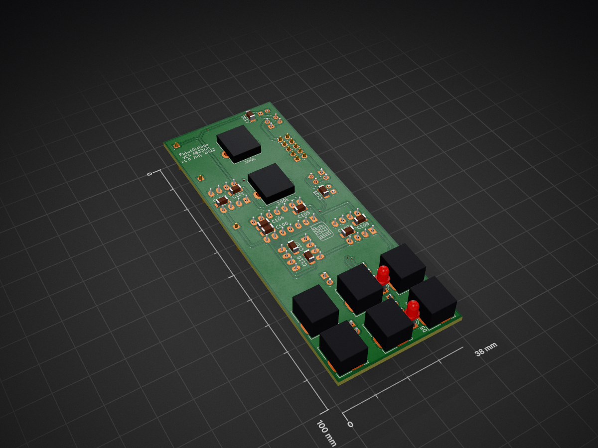
2 layers38 × 100 mmVca as3360-circuit, the printed circuit board in 3D

Vca as3360-circuit

fledsbo/Modules3

Eurorack module designs using KiCad — VCO, VCF, VCA, ADSR, and Daisy Seed

Size
38 × 100 mm
Copper layers
2
Thickness
1.6 mm
Parts
74
Nets
56
Pads
191
Tracks, vias
313, 6
Pours
1
Routed
Yes
KiCad
KiCad 6 (file 20211014)
Created
12 Apr 2026
Updated
12 Apr 2026

Overview

Vca as3360-circuit is an open-source printed circuit board by fledsbo, from the fledsbo/Modules repository on GitHub. It is a 2-layer board of 38 × 100 mm with 74 parts on 56 nets, routed with 313 tracks and 6 vias.

It is built around the TL072, LM358 and BC547. Its parts include 32 resistors, 13 capacitors, 10 connectors, 6 diodes and 4 ICs. It belongs with the audio and music boards of this library.

Main components

3

README

README.md

Eurorack Modules

A collection of Eurorack module designs using KiCad. Each module has separate KiCad projects for the circuit PCB and the front panel.

Modules

daisy-seed-multi — Digital Multi-Purpose Module

  • Core: Electrosmith Daisy Seed
  • Description: Programmable digital module — function determined by firmware (oscillator, effects, sequencer, etc.)
  • Based on: fablabnk/DaisyDelayHardware (KiCad 6+ project)
    • Includes Eurorack power, audio I/O with level shifting, CV inputs, pots, and custom footprints
    • See notes_schematic.md and notes_pcb.md for design rationale

vco-as3340 — Voltage Controlled Oscillator

vcf-as3320 — Voltage Controlled Filter

  • Core IC: AS3320 (CEM3320 clone)
  • Reference design: hermflink's 3320VCF
  • Based on: hermflink/3320VCF (GPL-3.0 license, legacy KiCad format)
    • ⚠️ Legacy KiCad format (.sch/.pro) — open in KiCad 8 to auto-convert to modern format
    • Multimode filter: 24dB LP, 12dB BP, 6dB HP+18dB LP, 6dB LP+6dB HP+12dB LP
    • Designed for ±15V but works with ±12V

vca-as3360 — Voltage Controlled Amplifier

  • Core IC: AS3360 (CEM3360 clone, dual VCA)
  • Reference design: Kassutronics Dual VCA / LMNC 1181
  • Based on: EchelonForce/vca_as3360 (CC-BY-NC-SA, KiCad 6+ project)
    • Hierarchical schematic (input block, output block, VCO block sub-sheets)
    • Includes front panel designs (FreeCAD .FCStd, DXF, SVG, PDF, and STEP files)

adsr-as3310 — ADSR Envelope Generator

Project Structure

Each module folder contains two KiCad projects:

  • circuit/ — main electronics PCB
  • panel/ — front panel PCB (for PCB-based panels)

The VCF uses legacy KiCad format and should be opened in KiCad 8 for automatic conversion.

Getting Started: Schematic to PCB Workflow

If you're new to KiCad, here's the recommended step-by-step process for turning a schematic into a finished PCB layout.

1. Review and Edit the Schematic

Open the .kicad_sch file in KiCad's Schematic Editor.

  • Read through the circuit and make sure you understand what each section does. The reference design blog posts (linked above) are invaluable for this.
  • Make any changes you want — swap component values, add/remove jacks, change pot tapers, etc.
  • Assign footprints to every component (Tools → Assign Footprints). Each symbol needs a physical footprint that matches the real part you'll solder. For example:
    • Resistors → Resistor_THT:R_Axial_DIN0207_L6.3mm_D2.5mm_P10.16mm_Horizontal (typical through-hole)
    • DIP ICs → Package_DIP:DIP-16_W7.62mm (check your IC's pin count)
    • 3.5mm jacks → Connector_Audio:Jack_3.5mm_QingPu_WQP-PJ398SM_Vertical (Thonkiconn, the Eurorack standard)
    • Potentiometers → Potentiometer_THT:Potentiometer_Alpha_RD901F-40-00D_Single_Vertical
  • Run Electrical Rules Check (Inspect → Electrical Rules Check) and fix any errors before proceeding.

2. Import Components into the PCB Editor

Open the PCB Editor (.kicad_pcb) and press F8 (or Tools → Update PCB from Schematic).

  • This imports all your components as a pile of footprints with a "rats nest" of thin lines showing which pads need to be connected.
  • Click OK to accept — don't worry, it looks like a mess at first. That's normal.

3. Define the Board Outline

Before placing components, draw the board outline on the Edge.Cuts layer.

  • For Eurorack, the board height is 128.5mm (the 3U standard).
  • Board width depends on your module's HP: 1 HP = 5.08mm. Common sizes:
    • 8 HP = 40.64mm
    • 10 HP = 50.80mm
    • 12 HP = 60.96mm
    • 14 HP = 71.12mm
  • Use Place → Rectangle on the Edge.Cuts layer, or draw lines with the Draw Line tool.
  • Add mounting holes at the standard Eurorack positions (3mm holes, 3.2mm from the top/bottom edges, 7.5mm from the left/right edges).

4. Place Components — The Most Important Step

Good placement is 90% of a good PCB. Take your time here.

General strategy:

  1. Start with connectors and mechanical parts — place the Eurorack power header, jacks, pots, and switches first. These are constrained by the front panel layout and physical access.
  2. Group related components together — keep each functional block (e.g., the expo converter, the waveform shapers, the output buffers) in its own area.
  3. Follow the signal flow — arrange components so the signal path flows logically across the board (typically left-to-right or top-to-bottom). This makes routing easier and reduces noise.
  4. Keep the main IC central — the AS3340/AS3320/AS3360/AS3310 should be near the middle of its associated circuitry.
  5. Place decoupling capacitors right next to their IC's power pins — this is critical for noise performance. Within 5mm, as close as physically possible.

Analog audio tips:

  • Keep audio signal traces away from digital signals and power traces.
  • Keep input and output sections on opposite sides of the board to prevent feedback.
  • Leave room for a ground plane (see step 6).

5. Route the Traces

Now connect all the pads according to the rats nest lines.

  • Press X to start routing a trace. KiCad's interactive router will push other traces out of the way.
  • Recommended trace widths:
    • Signal traces: 0.25–0.3mm (fine for audio and CV)
    • Power traces (+12V, -12V): 0.5–0.8mm (carry more current)
    • Ground: 0.5mm+ or use a ground plane (see below)
  • Route critical signals first:
    1. Ground connections
    2. Power (+12V, -12V)
    3. Audio signal paths (keep these short and direct)
    4. CV and control signals
  • Use 45° angles (KiCad's default) — avoid 90° corners on signal traces.
  • Use vias to switch between front and back copper layers when traces need to cross.
  • If you get stuck on a difficult route, try moving components slightly — often a small placement adjustment makes routing much easier.

6. Add a Ground Plane

A ground plane dramatically improves noise performance for analog audio circuits.

  • Select the back copper layer (B.Cu)
  • Place → Add Filled Zone → select the GND net → draw a rectangle covering the entire board
  • Press B to fill the zone
  • This connects all ground pads through a continuous copper pour, reducing ground loops and EMI.
  • You can add a ground plane on the front (F.Cu) too, but leave enough clearance around signal traces.

7. Run Design Rule Check (DRC)

Before ordering, run Inspect → Design Rules Check to catch:

  • Unconnected nets (missed connections)
  • Clearance violations (traces too close together)
  • Missing footprints
  • Courtyard overlaps (components physically overlapping)

Fix every error. Warnings can sometimes be acceptable — review them individually.

8. Generate Manufacturing Files

When your layout is complete and DRC passes:

  1. Gerber files: File → Fabrication Outputs → Gerbers — these are what the PCB manufacturer needs
    • Include: F.Cu, B.Cu, F.SilkS, B.SilkS, F.Mask, B.Mask, Edge.Cuts
    • Also generate the drill file (File → Fabrication Outputs → Drill Files)
  2. Review in Gerber Viewer: Inspect → Gerber Viewer or use an online viewer like Tracespace to double-check before ordering
  3. Upload to your fab — JLCPCB, PCBWay, OSH Park, etc. all accept KiCad Gerber output directly

9. Front Panel PCB

Each module also has a panel/ folder for designing the front panel as a PCB:

  • Create a board outline matching the module's HP width × 128.5mm height
  • Add cutouts for jacks, pots, switches, and LEDs as mounting holes or non-plated through-holes (NPTH)
  • Add labels and graphics on the F.SilkS (silkscreen) layer for a professional look
  • Standard Eurorack mounting slots: oval holes (3.2mm × 4mm) at top and bottom, centered at 3mm from each horizontal edge
  • Order with a different solder mask color than your circuit board for visual distinction (e.g., black panel, green circuit board)

Using Freerouting for Auto-Routing (Optional)

KiCad doesn't have a built-in autorouter, but you can use Freerouting:

  1. In KiCad PCB Editor: File → Export → Specctra DSN
  2. Open the .dsn file in Freerouting → click "Autoroute"
  3. Export the result as a .ses (Specctra Session) file
  4. Back in KiCad: File → Import → Specctra Session

Caveat: Autorouting works best for digital boards. For analog audio modules, you'll likely want to hand-route critical audio paths and use the autorouter only for less-sensitive connections like power distribution and LED indicators.

Notes

  • All modules target standard Eurorack format (3U height, ±12V power)
  • Panel width (HP) to be determined per module
  • Source projects are used as starting points — modify and adapt as needed

Parts

74
QtyValueFootprintReferences
16100kResistor_SMD:R_1206_3216Metric_Pad1.30x1.75mm_HandSolderR3, R5, R6, R9, R10, R11, R13, R14, R16, R17, R18, R21, R22, R23, R26, R31
1110nFCapacitor_SMD:C_1206_3216Metric_Pad1.33x1.80mm_HandSolderC100, C101, C102, C103, C104, C105, C106, C107, C108, C109, C110
61kResistor_SMD:R_1206_3216Metric_Pad1.30x1.75mm_HandSolderR15, R25, R27, R28, R30, R32
410kResistor_SMD:R_1206_3216Metric_Pad1.30x1.75mm_HandSolderR1, R2, R7, R8
4DDiode_THT:D_A-405_P2.54mm_Vertical_KathodeUpD2, D3, D4, D6
2100kMy Stuff:Potentiometer_Alpha_RD901F-40-00D_Single_Vertical_w_3dRV1, RV2
2100uFCapacitor_THT:CP_Radial_D5.0mm_P2.50mmC2, C3
2400kResistor_SMD:R_1206_3216Metric_Pad1.30x1.75mm_HandSolderR24, R29
247kResistor_SMD:R_1206_3216Metric_Pad1.30x1.75mm_HandSolderR4, R12
250kResistor_SMD:R_1206_3216Metric_Pad1.30x1.75mm_HandSolderR19, R20
2BC547Package_TO_SOT_THT:TO-92_Inline_WideQ1, Q2
2FerriteBeadInductor_THT:L_Axial_L6.6mm_D2.7mm_P2.54mm_Vertical_Vishay_IM-2FB1, FB2
2TL072Package_DIP:DIP-8_W7.62mm_Socket_LongPadsU1, U4
1+12VConnector_PinHeader_2.54mm:PinHeader_1x01_P2.54mm_VerticalJ1
1-12VConnector_PinHeader_2.54mm:PinHeader_1x01_P2.54mm_VerticalJ9
1AS3360Package_DIP:DIP-14_W7.62mm_Socket_LongPadsU2
1CV 1 LEDLED_THT:LED_D3.0mmD1
1CV 2 LEDLED_THT:LED_D3.0mmD5
1CV1My Stuff:Jack_3.5mm_MJ-355W_VerticalJ4
1CV2My Stuff:Jack_3.5mm_MJ-355W_VerticalJ5
1Conn_02x05_Odd_EvenConnector_IDC:IDC-Header_2x05_P2.54mm_VerticalJ8
1GNDConnector_PinHeader_2.54mm:PinHeader_1x01_P2.54mm_VerticalJ10
1IN1My Stuff:Jack_3.5mm_MJ-355W_VerticalJ6
1IN2My Stuff:Jack_3.5mm_MJ-355W_VerticalJ7
1LM358Package_DIP:DIP-8_W7.62mm_Socket_LongPadsU3
1Logo_Open_Hardware_SmallSymbol:OSHW-Symbol_6.7x6mm_SilkScreenLOGO100
1OUT_1My Stuff:Jack_3.5mm_MJ-355W_VerticalJ2
1OUT_2My Stuff:Jack_3.5mm_MJ-355W_VerticalJ3
1logo1My Stuff:Logo2LOGO102
1logo1My Stuff:Logo1LOGO101

Questions

How big is the Vca as3360-circuit PCB?

It measures 38 × 100 mm and has 2 copper layers, 1.6 mm thick.

What parts does the Vca as3360-circuit use?

74 parts, built around the TL072, LM358 and BC547. The full list of its parts is on this page, with links to each part's symbol and footprint where PCBKit's library has them.

Where can I download the Vca as3360-circuit KiCad files?

From the fledsbo/Modules repository on GitHub, at the commit this page was made from: the board is vca-as3360/circuit/vca-as3360-circuit.kicad_pcb and its schematic adsr-as3310/circuit/adsr-as3310-circuit.kicad_sch. PCBKit opens the board in the browser, with nothing to install.

Can I use the Vca as3360-circuit design in my own project?

Its repository states no licence, so its author keeps all rights: ask fledsbo before reusing the design.

Similar boards

  • 2 layers76 × 100 mmVclfo10, the printed circuit board in 3D

    Vclfo10

    EchelonForce/vclfo10

    A Eurorack LFO design based on the Electric Druid VCLFO10 chip.

    139 parts7
  • 4 layers140 × 136 mmVinyl adc rev d, the printed circuit board in 3D

    Vinyl adc rev d

    MadsRudolph/vinyl-adc

    Discrete 3rd-order delta-sigma stereo audio ADC, built from op-amps and logic gates: a four-layer Raspberry Pi HAT made by PCBWay, with KiCad files, SPICE simulations and measurements

    184 parts1
  • 2 layers105 × 128.5 mmMiniADSR 1.1, the printed circuit board in 3D

    MiniADSR 1.1

    benjiaomodular/MiniADSR

    A 4HP envelope generator for Eurorack modular synth

    52 parts21MIT
  • 2 layers135.8 × 128.4 mmMoog Filter, the printed circuit board in 3D

    Moog Filter

    jojo-monk/Yusynth-MiniMoog-Filter

    Eurorack adaptation

    78 parts8
  • 2 layers67 × 100 mmLfo stomp v1 panelized, the printed circuit board in 3D

    Lfo stomp v1 panelized

    EchelonForce/lfo_stomp

    A design for a Eurorack LFO module based on the ElectricDruid STOMPLFO chip.

    100 parts5
  • 2 layers245.4 × 128.5 mmMOL, the printed circuit board in 3D

    MOL

    juanlittledevil/MOL

    Dual ADSR/VCA combo module for Eurorack

    210 parts4
  • 2 layers30.5 × 99.1 mmMinimoog, the printed circuit board in 3D

    Minimoog

    vk2gpu/eurorack-modules

    Collection of Eurorack module schematics

    74 parts4